- 您现在的位置:买卖IC网 > Datasheet目录996 > NCP5612GEVB (ON Semiconductor)EVAL BOARD FOR NCP5612G Datasheet资料下载
参数资料
| 型号: | NCP5612GEVB |
| 厂商: | ON Semiconductor |
| 文件页数: | 7/11页 |
| 文件大小: | 0K |
| 描述: | EVAL BOARD FOR NCP5612G |
| 设计资源: | NCP5612 EVB BOM NCP5612GEVB Gerber Files NCP5612 EVB Schematic NCP5612 BOM - V1.0 |
| 标准包装: | 1 |
| 电流 - 输出 / 通道: | 60mA |
| 输出及类型: | 2,非隔离 |
| 输出电压: | 4.8 ~ 5.7 V |
| 特点: | 亮度控制 |
| 输入电压: | 3.6V |
| 已供物品: | 板 |
| 已用 IC / 零件: | NCP5612 |
| 其它名称: | NCP5612GEVBOS |
�� �
�
�NCP5612�
�VBandGap�
�LED� Return�
�Pin� 2� &� 3�
�600� mV�
�R1�
�I� REF�
�Pin� 4�
�GND�
�GND�
�Note:� the� I� REF� pin� must� never� be� biased� by� an� external� voltage.�
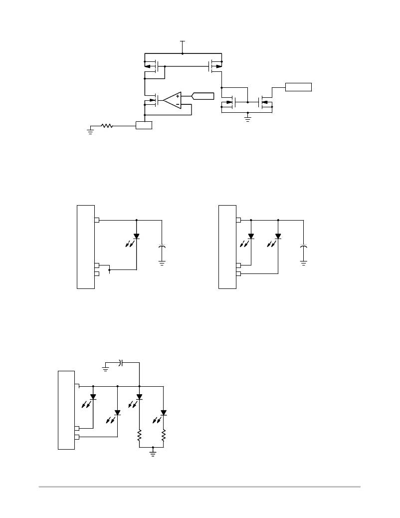
�Figure� 5.� Basic� Reference� Current� Source�
�Load� Connection�
�The� NCP5612� is� capable� to� drive� the� two� LED�
�simultaneously,� as� depicted� (see� Figure� 1),� but� the� load� can�
�be� arranged� to� accommodate� one� or� two� LED� if� necessary�
�NCP5612�
�7�
�in� the� application� (see� Figure� 6).� In� this� case,� the� two�
�current� mirrors� can� be� connected� in� parallel� to� drive� a�
�single� powerful� LED,� thus� yielding� 60� mA� current�
�capability� in� a� single� LED.�
�NCP5612�
�7�
�LWY87S�
�D1�
�LWY87S�
�LWY87S�
�D1�
�C4�
�1� m� F/6.3� V�
�D2�
�C4�
�1� m� F/6.3� V�
�2�
�3�
�GND�
�2�
�3�
�GND�
�Figure� 6.� Typical� Single� and� Double� LED� Connections�
�Finally,� an� external� network� can� be� connected� across� V� out�
�and� ground,� but� the� current� through� such� network� will� not�
�be� regulated� by� the� NCP5612� chip� (see� Figure� 7).� On� top�
�of� that,� the� total� current� out� of� the� V� out� pin� shall� be� limited�
�to� 60� mA.�
�C4�
�Single� Wire� Serial� Link� Protocol�
�The� proposed� S?WIRE� uses� a� pulse� count� technique�
�already� existing� in� the� data� exchange� systems.� The� protocol�
�supports� broken� transmission,� assuming� the� hold� time� is�
�shorter� than� the� maximum� 200� m� s� typical� specified� in� the�
�data� sheet.� The� S?WIRE� details� are� provided� in� the�
�AND8264� application� note.�
�NCP5612�
�7�
�GND�
�1uF/6.3V�
�Based� on� the� two� examples� provided� in� Figure� 8,� the�
�CNTL� pin� supports� two� digital� level:�
�CNTL� =� Low� 3� the� system� is� shut?off� and� no� current�
�D1�
�LWY87S�
�D3�
�LWY87S�
�flow� in� either� LED1� or� LED2.�
�CNTL� =� High� 3� the� system� is� active� and� the� two� LED�
�20� mA�
�2�
�LWY87S�
�20� mA�
�D2�
�5mA�
�R1�
�LWY87S�
�5mA�
�D4�
�R2�
�are� powered� according� to� the� selected� sequence.�
�There� is� no� time� delay� associated� with� the� Low� state� and�
�the� LED� are� switched� Off� when� the� CNTL� signal� drops� to�
�Low.� To� program� a� new� LED� configuration,� one� shall� send�
�3�
�220R�
�GND�
�220R�
�the� number� of� pulses� on� the� CNTL� pin� according� to� the� true�
�table:�
�?� The� internal� counter� is� reset� to� zero� on� the� first�
�negative� going� transient� present� on� the� CNTL� pin�
�Figure� 7.� Extra� Load� Connected� to� V� out�
�http://onsemi.com�
�7�
�相关PDF资料 |
PDF描述 |
|---|---|
| NCV7680PWR22GEVB | BOARD EVALUATION NCV7680 |
| NDNA200 | DIN-RAIL 35MM ALUMINUM 2M |
| NG-9517 | CABLE GLAND NEMA 4X PG-29 BLACK |
| NH2503K000FJ01 | 250WATTS 3KOHMS 1% NON-INDUCTIVE |
| NHN0.50BK | GORILLA SLEEVING 1/2" BLACK 500' |
相关代理商/技术参数 |
参数描述 |
|---|---|
| NCP5612MUTBG | 功能描述:LED照明驱动器 WHITE LED DRIVER- 2LED-SW RoHS:否 制造商:STMicroelectronics 输入电压:11.5 V to 23 V 工作频率: 最大电源电流:1.7 mA 输出电流: 最大工作温度: 安装风格:SMD/SMT 封装 / 箱体:SO-16N |
| NCP561SN15T1 | 功能描述:低压差稳压器 - LDO 1.5V 150mA CMOS RoHS:否 制造商:Texas Instruments 最大输入电压:36 V 输出电压:1.4 V to 20.5 V 回动电压(最大值):307 mV 输出电流:1 A 负载调节:0.3 % 输出端数量: 输出类型:Fixed 最大工作温度:+ 125 C 安装风格:SMD/SMT 封装 / 箱体:VQFN-20 |
| NCP561SN15T1G | 功能描述:低压差稳压器 - LDO 1.5V 150mA CMOS w/Enable RoHS:否 制造商:Texas Instruments 最大输入电压:36 V 输出电压:1.4 V to 20.5 V 回动电压(最大值):307 mV 输出电流:1 A 负载调节:0.3 % 输出端数量: 输出类型:Fixed 最大工作温度:+ 125 C 安装风格:SMD/SMT 封装 / 箱体:VQFN-20 |
| NCP561SN18T1 | 功能描述:低压差稳压器 - LDO 1.8V 150mA CMOS RoHS:否 制造商:Texas Instruments 最大输入电压:36 V 输出电压:1.4 V to 20.5 V 回动电压(最大值):307 mV 输出电流:1 A 负载调节:0.3 % 输出端数量: 输出类型:Fixed 最大工作温度:+ 125 C 安装风格:SMD/SMT 封装 / 箱体:VQFN-20 |
| NCP561SN18T1G | 功能描述:低压差稳压器 - LDO 1.8V 150mA CMOS w/Enable RoHS:否 制造商:Texas Instruments 最大输入电压:36 V 输出电压:1.4 V to 20.5 V 回动电压(最大值):307 mV 输出电流:1 A 负载调节:0.3 % 输出端数量: 输出类型:Fixed 最大工作温度:+ 125 C 安装风格:SMD/SMT 封装 / 箱体:VQFN-20 |
发布紧急采购,3分钟左右您将得到回复。