- 您现在的位置:买卖IC网 > PDF目录20815 > NCP5612MUTBG (ON Semiconductor)IC WHITE LED DRVR 12-LLGA PDF资料下载
参数资料
| 型号: | NCP5612MUTBG |
| 厂商: | ON Semiconductor |
| 文件页数: | 6/11页 |
| 文件大小: | 0K |
| 描述: | IC WHITE LED DRVR 12-LLGA |
| 标准包装: | 1 |
| 拓扑: | 切换式电容器(充电泵) |
| 输出数: | 2 |
| 内部驱动器: | 是 |
| 类型 - 主要: | 背光,闪灯/白光 |
| 类型 - 次要: | 白色 LED |
| 频率: | 1MHz |
| 电源电压: | 2.7 V ~ 5.5 V |
| 输出电压: | 4.8 V ~ 5.7 V |
| 安装类型: | 表面贴装 |
| 封装/外壳: | 12-UFLGA 裸露焊盘 |
| 供应商设备封装: | 12-LLGA(2x2) |
| 包装: | 剪切带 (CT) |
| 工作温度: | -40°C ~ 85°C |
| 其它名称: | NCP5612MUTBGOSCT |
�� �
�
�NCP5612�
�APPLICATION� INFORMATION�
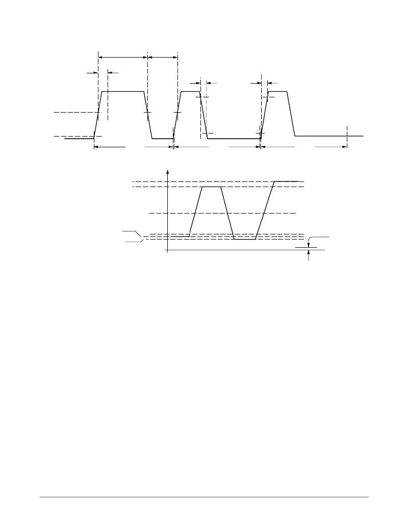
�t� wkp�
�t� on�
�t� off�
�V� IH�
�t� f�
�90%�
�t� r�
�90%�
�V� IL�
�10%�
�Bit� =� 1�
�Bit� =� 0�
�Bit� =� 0�
�Figure� 3.� Timings� Reference�
�V� OH� @� V� ccio� =� 3.0� V� 2600� mV�
�V� OH� @� V� ccio� =� 2.6� V� 2400� mV�
�1400� mV�
�V� IHsw�
�V� OL� @� MOTOROLA:� 500� mV�
�V� OL� @� QUALCOMM:� 450� mV�
�V� OL� @� INTEL:� 400� mV�
�V� IL�
�600� mV�
�100� mV/step�
�GROUND�
�Figure� 4.� Basic� Cellular� Phone� Chip� Set� Digital� Output� Levels�
�DC/DC� Operation�
�The� converter� is� based� on� a� charge� pump� technique� to�
�generate� a� DC� voltage� capable� to� supply� the� White� LED�
�load.� The� system� regulates� the� current� flowing� into� each�
�LED� by� means� of� internal� current� mirrors� associated� with�
�the� white� diodes.� Consequently,� the� output� voltage� will� be�
�equal� to� the� V� f� of� the� LED,� plus� the� drop� voltage� (ranging�
�from� 150� mV� to� 400� mV,� depending� upon� the� output�
�current� and� V� bat� /� V� f� ratio)� developed� across� the� internal�
�NMOS� mirror.� Typically,� assuming� a� standard� white� LED�
�forward� biased� at� 10� mA,� the� output� voltage� will� be� 3.6� V.�
�The� built?in� OVP� circuit� continuously� monitors� the�
�output� voltage� and� stops� the� converter� when� the� voltage� is�
�above� 5.0� V� typical.� The� converter� resumes� to� normal�
�operation� when� the� voltage� drops� below� the� typical� 5.0� V�
�(no� latch?up� mechanism).� Consequently,� the� chip� can�
�operate� with� no� load� during� any� test� procedures.�
�Load� Current� Calculation�
�The� load� current� is� derived� from� the� 600� mV� reference�
�voltage� provided� by� the� internal� Band� Gap� associated� to� the�
�external� resistor� connected� across� I� REF� pin� and� Ground� (see�
�Figure� 5).� In� any� case,� no� voltage� shall� be� forced� at� I� REF� pin,�
�either� downward� or� upward.�
�The� reference� current� is� multiplied� by� the� internal�
�current� mirror,� associated� to� the� number� of� pulses� as�
�depicted� Figure� 9,� to� yield� the� output� load� current.� Since� the�
�reference� voltage� is� based� on� a� temperature� compensated�
�Band� Gap,� a� tight� tolerance� resistor� will� provide� a� very�
�accurate� load� current.� The� resistor� is� calculated� from� the�
�Ohm’s� law� (R� bias� =� V� ref� /I� REF� )� and� define� the� maximum�
�current� flowing� into� the� LED� when� 20� pulses� have� been�
�counted� at� the� CNTL� pin.�
�Since� the� reference� current� must� be� between� the�
�minimum� and� maximum� specified,� the� resistor� value� will�
�range� between� R� bias� =� 300/30� mA� =� 10� k� W� and� R� bias� =�
�300/0.5� mA� =� 600� k� W� .� Obviously,� the� tolerance� of� such� a�
�resistor� must� be� 1%� or� better,� with� a� 100� ppm� thermal�
�coefficient,� to� get� the� expected� overall� tolerance.�
�Typical� applications� will� run� with� R� bias� =� 10� k� W� to� make�
�profit� of� the� full� dynamic� range� provided� by� the� S?Wire�
�DATA� byte.�
�http://onsemi.com�
�6�
�相关PDF资料 |
PDF描述 |
|---|---|
| F971C106MBA | CAP TANT 10UF 16V 20% SMD |
| P51-3000-S-T-M12-4.5V-000-000 | SENSOR 3000PSI 7/16-20-2B 4.5V |
| REC3-2405DRW/H6/C/SMD-R | CONV DC/DC 3W 18-36VIN +/-05VOUT |
| REC8-1205DRW/H2/A/M/SMD-R | CONV DC/DC 8W 12VIN +/-05VOUT |
| P51-200-S-AA-P-5V-000-000 | SENSOR 200PSIS 7/16 UNF 5V |
相关代理商/技术参数 |
参数描述 |
|---|---|
| NCP561SN15T1 | 功能描述:低压差稳压器 - LDO 1.5V 150mA CMOS RoHS:否 制造商:Texas Instruments 最大输入电压:36 V 输出电压:1.4 V to 20.5 V 回动电压(最大值):307 mV 输出电流:1 A 负载调节:0.3 % 输出端数量: 输出类型:Fixed 最大工作温度:+ 125 C 安装风格:SMD/SMT 封装 / 箱体:VQFN-20 |
| NCP561SN15T1G | 功能描述:低压差稳压器 - LDO 1.5V 150mA CMOS w/Enable RoHS:否 制造商:Texas Instruments 最大输入电压:36 V 输出电压:1.4 V to 20.5 V 回动电压(最大值):307 mV 输出电流:1 A 负载调节:0.3 % 输出端数量: 输出类型:Fixed 最大工作温度:+ 125 C 安装风格:SMD/SMT 封装 / 箱体:VQFN-20 |
| NCP561SN18T1 | 功能描述:低压差稳压器 - LDO 1.8V 150mA CMOS RoHS:否 制造商:Texas Instruments 最大输入电压:36 V 输出电压:1.4 V to 20.5 V 回动电压(最大值):307 mV 输出电流:1 A 负载调节:0.3 % 输出端数量: 输出类型:Fixed 最大工作温度:+ 125 C 安装风格:SMD/SMT 封装 / 箱体:VQFN-20 |
| NCP561SN18T1G | 功能描述:低压差稳压器 - LDO 1.8V 150mA CMOS w/Enable RoHS:否 制造商:Texas Instruments 最大输入电压:36 V 输出电压:1.4 V to 20.5 V 回动电压(最大值):307 mV 输出电流:1 A 负载调节:0.3 % 输出端数量: 输出类型:Fixed 最大工作温度:+ 125 C 安装风格:SMD/SMT 封装 / 箱体:VQFN-20 |
| NCP561SN25T1 | 功能描述:低压差稳压器 - LDO 2.5V 150mA CMOS RoHS:否 制造商:Texas Instruments 最大输入电压:36 V 输出电压:1.4 V to 20.5 V 回动电压(最大值):307 mV 输出电流:1 A 负载调节:0.3 % 输出端数量: 输出类型:Fixed 最大工作温度:+ 125 C 安装风格:SMD/SMT 封装 / 箱体:VQFN-20 |
发布紧急采购,3分钟左右您将得到回复。