- 您现在的位置:买卖IC网 > PDF目录22211 > NCP582DXV15T2G (ON Semiconductor)IC REG LDO 1.5V .15A SOT-563 PDF资料下载
参数资料
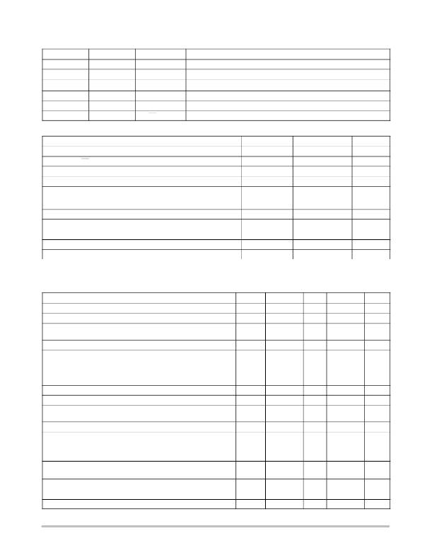
| 型号: | NCP582DXV15T2G |
| 厂商: | ON Semiconductor |
| 文件页数: | 2/12页 |
| 文件大小: | 0K |
| 描述: | IC REG LDO 1.5V .15A SOT-563 |
| 标准包装: | 4,000 |
| 稳压器拓扑结构: | 正,固定式 |
| 输出电压: | 1.5V |
| 输入电压: | 2 V ~ 6 V |
| 电压 - 压降(标准): | 0.38V @ 150mA |
| 稳压器数量: | 1 |
| 电流 - 输出: | 150mA(最小) |
| 工作温度: | -40°C ~ 85°C |
| 安装类型: | 表面贴装 |
| 封装/外壳: | SOT-563,SOT-666 |
| 供应商设备封装: | SOT-563 |
| 包装: | 带卷 (TR) |
�� �
�
�NCP582�
�PIN FUNCTIO� N� DESCRIPTION�
�SOT� ?� 563� Pin�
�1�
�2�
�3�
�4�
�5�
�6�
�SC� ?� 82AB� Pin�
�4�
�2�
�3�
�?�
�?�
�1�
�Symbol�
�Vin�
�GND�
�Vout�
�NC�
�GND�
�CE� or� CE�
�Power� supply� inout� voltage.�
�Power� supply� ground.�
�Regulated� output� voltage.�
�No� connect.�
�Power� supply� ground.�
�Chip� enable� pin.�
�Description�
�MAXIMUM� RATINGS�
�Rating�
�Input� Voltage�
�Input� Voltage� (CE� or� CE� Pin)�
�Output� Voltage�
�Output� Current�
�Power� Dissipation�
�SC� ?� 82AB�
�SOT� ?� 563�
�ESD� Capability,� Human� Body� Model,� C� =� 100� pF,� R� =� 1.5� k� W�
�ESD� Capability,� Machine� Model,� C� =� 200� pF,� R� =� 0� W�
�Operating� Ambient� Temperature� Range�
�Maximum� Junction� Temperature�
�Storage� Temperature� Range�
�Symbol�
�V� in�
�V� CE�
�V� out�
�I� out�
�P� D�
�ESD� HBM�
�ESD� MM�
�T� A�
�T� J(max)�
�T� stg�
�Value�
�6.5�
�?� 0.3� to� V� in� +0.3�
�?� 0.3� to� V� in� +0.3�
�200�
�150�
�500�
�2000�
�200�
�?� 40� to� +85�
�125�
�?� 55� to� +150�
�Unit�
�V�
�V�
�V�
�mA�
�mW�
�V�
�V�
�°� C�
�°� C�
�°� C�
�Stresses� exceeding� Maximum� Ratings� may� damage� the� device.� Maximum� Ratings� are� stress� ratings� only.� Functional� operation� above� the�
�Recommended� Operating� Conditions� is� not� implied.� Extended� exposure� to� stresses� above� the� Recommended� Operating� Conditions� may� affect�
�device� reliability.�
�ELECTRICAL CHARACTERISTICS� (V� in� = V� out� + 1.0 V, T� A� = 25� °� C, unles s otherwise� noted.)�
�Characteristic�
�Input� Voltage�
�Output� Voltage� (I� out� =� 1.0� mA� to� 30� mA)�
�Symbol�
�V� in�
�V� out�
�Min�
�2.0�
�V� out� X� 0.980�
�Typ�
�?�
�?�
�Max�
�6.0�
�V� out� X� 1.020�
�Unit�
�V�
�V�
�Line� Regulation� (I� out� =� 30� mA),�
�(V� out� >� 1.7� V;� V� out� +� 0.5� V� v� V� in� v� 6.0� V)�
�(V� out� =� 1.5� V;� 2.2� V� v� V� in� v� 6.0� V)�
�Reg� line�
�?�
�0.02�
�0.10�
�%/V�
�Load� Regulation� (I� out� =� 1.0� mA� to� 150� mA)�
�Dropout� Voltage� (I� out� =� 150� mA)�
�V� out� =� 1.5� V�
�V� out� =� 1.8� V�
�V� out� =� 2.5� V�
�2.8� V� v� V� out� v� 3.3� V�
�Quiescent� Current� (I� out� =� 0� mA)�
�Output� Current�
�Shutdown� Current� (V� CE� =� Gnd� for� Active� High� with� Auto� Discharge)�
�(V� CE� =� V� in� for� Active� Low)�
�Output� Short� Circuit� Current� (V� out� =� 0)�
�Reg� load�
�V� DO�
�Iq�
�I� out�
�I� SD�
�I� lim�
�?�
�?�
�?�
�?�
�?�
�?�
�150�
�?�
�?�
�22�
�0.38�
�0.32�
�0.28�
�0.22�
�75�
�?�
�0.1�
�40�
�40�
�0.70�
�0.55�
�0.50�
�0.35�
�95�
�?�
�1.0�
�?�
�mV�
�V�
�m� A�
�mA�
�m� A�
�mA�
�Ripple� Rejection� (I� out� =� 30� mA)�
�Enable� Input� Threshold� Voltage�
�(V� out� >� 1.7� V;� V� in� –� V� out� =� 1.0� V)�
�(V� out� =� 1.5� V;� V� in� –� V� out� =� 1.2� V)�
�f� =� 1.0� kHz�
�f� =� 10� kHz�
�High�
�Low�
�RR�
�Vth� enh�
�Vth� enl�
�?�
�?�
�1.5�
�0�
�70�
�60�
�?�
�?�
�?�
�?�
�V� in�
�0.3�
�dB�
�V�
�Output� Noise� Voltage� (Bandwidth� =� 10� Hz� to� 100� kHz)�
�Output� Voltage� Temperature� Coefficient� (I� out� =� 30� mA,� ?� 40� °� C� v� T� A� v� 85� °� C)�
�N� ?� Channel� On� Resistance� for� Auto� Discharge�
�V� n�
�D� V� out� /� D� T�
�R� Low�
�?�
�?�
�?�
�30�
�"� 100�
�60�
�?�
�?�
�?�
�m� Vrms�
�ppm/� °� C�
�W�
�http://onsemi.com�
�2�
�相关PDF资料 |
PDF描述 |
|---|---|
| ABM28DSXI | CONN EDGECARD 56POS DIP .156 SLD |
| GMC08DRES-S13 | CONN EDGECARD 16POS .100 EXTEND |
| GBC07DREF-S13 | CONN EDGECARD 14POS .100 EXTEND |
| AMM15DRYS | CONN EDGECARD 30POS DIP .156 SLD |
| PM3316-1R0M-RC | INDUCTOR POWER 1.0UH 7.5A SMD |
相关代理商/技术参数 |
参数描述 |
|---|---|
| NCP582DXV18T1G | 制造商:ON Semiconductor 功能描述:REG LDO LIN FIX POS 1.8V 0.15A 6PIN SOT-563 - Tape and Reel 制造商:Rochester Electronics LLC 功能描述: |
| NCP582DXV18T2G | 功能描述:低压差稳压器 - LDO 1.8V 150mA w/Enable RoHS:否 制造商:Texas Instruments 最大输入电压:36 V 输出电压:1.4 V to 20.5 V 回动电压(最大值):307 mV 输出电流:1 A 负载调节:0.3 % 输出端数量: 输出类型:Fixed 最大工作温度:+ 125 C 安装风格:SMD/SMT 封装 / 箱体:VQFN-20 |
| NCP582DXV25T1G | 制造商:ON Semiconductor 功能描述:REG LDO LIN FIX POS 2.5V 0.15A 6PIN SOT-563 - Tape and Reel |
| NCP582DXV25T2G | 功能描述:低压差稳压器 - LDO 2.5V 150mA w/Enable RoHS:否 制造商:Texas Instruments 最大输入电压:36 V 输出电压:1.4 V to 20.5 V 回动电压(最大值):307 mV 输出电流:1 A 负载调节:0.3 % 输出端数量: 输出类型:Fixed 最大工作温度:+ 125 C 安装风格:SMD/SMT 封装 / 箱体:VQFN-20 |
| NCP582DXV28T1G | 制造商:ON Semiconductor 功能描述:REG LDO LIN FIX POS 2.8V 0.15A 6PIN SOT-563 - Tape and Reel |
发布紧急采购,3分钟左右您将得到回复。