参数资料
| 型号: | NCV2002SN1T1 |
| 厂商: | ON Semiconductor |
| 文件页数: | 8/16页 |
| 文件大小: | 0K |
| 描述: | IC OPAMP R-R 0.9V 1A 6-TSOP |
| 产品变化通告: | Product Obsolescence 11/Feb/2009 |
| 标准包装: | 3,000 |
| 放大器类型: | 通用 |
| 电路数: | 1 |
| 输出类型: | 满摆幅 |
| 转换速率: | 1.3 V/µs |
| 增益带宽积: | 900kHz |
| 电流 - 输入偏压: | 10pA |
| 电压 - 输入偏移: | 500µV |
| 电流 - 电源: | 820µA |
| 电流 - 输出 / 通道: | 128mA |
| 电压 - 电源,单路/双路(±): | 0.9 V ~ 7 V,±0.45 V ~ 3.5 V |
| 工作温度: | -40°C ~ 125°C |
| 安装类型: | 表面贴装 |
| 封装/外壳: | SC-74,SOT-457 |
| 供应商设备封装: | 6-TSOP |
| 包装: | 带卷 (TR) |
NCS2002, NCV2002
http://onsemi.com
16
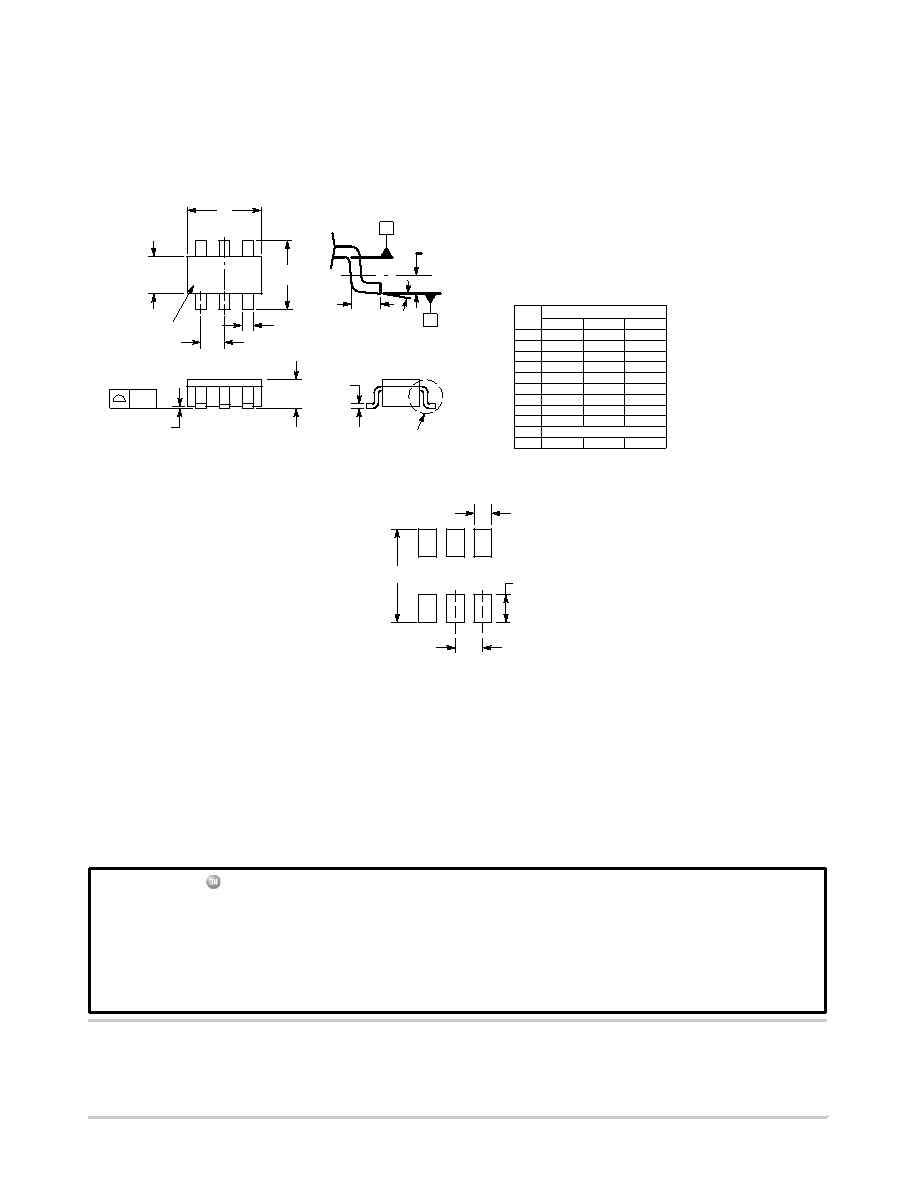
PACKAGE DIMENSIONS
TSOP6
CASE 318G02
ISSUE V
23
4
5
6
D
1
e
b
E1
A1
A
0.05
NOTES:
1. DIMENSIONING AND TOLERANCING PER ASME Y14.5M, 1994.
2. CONTROLLING DIMENSION: MILLIMETERS.
3. MAXIMUM LEAD THICKNESS INCLUDES LEAD FINISH. MINIMUM
LEAD THICKNESS IS THE MINIMUM THICKNESS OF BASE MATERIAL.
4. DIMENSIONS D AND E1 DO NOT INCLUDE MOLD FLASH,
PROTRUSIONS, OR GATE BURRS. MOLD FLASH, PROTRUSIONS, OR
GATE BURRS SHALL NOT EXCEED 0.15 PER SIDE. DIMENSIONS D
AND E1 ARE DETERMINED AT DATUM H.
5. PIN ONE INDICATOR MUST BE LOCATED IN THE INDICATED ZONE.
c
*For additional information on our PbFree strategy and soldering
details, please download the ON Semiconductor Soldering and
Mounting Techniques Reference Manual, SOLDERRM/D.
SOLDERING FOOTPRINT*
DIM
A
MIN
NOM
MAX
MILLIMETERS
0.90
1.00
1.10
A1
0.01
0.06
0.10
b
0.25
0.38
0.50
c
0.10
0.18
0.26
D
2.90
3.00
3.10
E
2.50
2.75
3.00
e
0.85
0.95
1.05
L
0.20
0.40
0.60
0.25 BSC
L2
0
°
10°
1.30
1.50
1.70
E1
E
RECOMMENDED
NOTE 5
L
C
M
H
L2
SEATING
PLANE
GAUGE
PLANE
DETAIL Z
0.60
6X
3.20
0.95
6X
0.95
PITCH
DIMENSIONS: MILLIMETERS
M
ON Semiconductor and
are registered trademarks of Semiconductor Components Industries, LLC (SCILLC). SCILLC owns the rights to a number of patents, trademarks,
copyrights, trade secrets, and other intellectual property. A listing of SCILLC’s product/patent coverage may be accessed at www.onsemi.com/site/pdf/PatentMarking.pdf. SCILLC
reserves the right to make changes without further notice to any products herein. SCILLC makes no warranty, representation or guarantee regarding the suitability of its products for any
particular purpose, nor does SCILLC assume any liability arising out of the application or use of any product or circuit, and specifically disclaims any and all liability, including without
limitation special, consequential or incidental damages. “Typical” parameters which may be provided in SCILLC data sheets and/or specifications can and do vary in different applications
and actual performance may vary over time. All operating parameters, including “Typicals” must be validated for each customer application by customer’s technical experts. SCILLC
does not convey any license under its patent rights nor the rights of others. SCILLC products are not designed, intended, or authorized for use as components in systems intended for
surgical implant into the body, or other applications intended to support or sustain life, or for any other application in which the failure of the SCILLC product could create a situation where
personal injury or death may occur. Should Buyer purchase or use SCILLC products for any such unintended or unauthorized application, Buyer shall indemnify and hold SCILLC and
its officers, employees, subsidiaries, affiliates, and distributors harmless against all claims, costs, damages, and expenses, and reasonable attorney fees arising out of, directly or indirectly,
any claim of personal injury or death associated with such unintended or unauthorized use, even if such claim alleges that SCILLC was negligent regarding the design or manufacture
of the part. SCILLC is an Equal Opportunity/Affirmative Action Employer. This literature is subject to all applicable copyright laws and is not for resale in any manner.
PUBLICATION ORDERING INFORMATION
N. American Technical Support: 8002829855 Toll Free
USA/Canada
Europe, Middle East and Africa Technical Support:
Phone: 421 33 790 2910
Japan Customer Focus Center
Phone: 81358171050
NCS2002/D
LITERATURE FULFILLMENT:
Literature Distribution Center for ON Semiconductor
P.O. Box 5163, Denver, Colorado 80217 USA
Phone: 3036752175 or 8003443860 Toll Free USA/Canada
Fax: 3036752176 or 8003443867 Toll Free USA/Canada
Email: orderlit@onsemi.com
ON Semiconductor Website: www.onsemi.com
Order Literature: http://www.onsemi.com/orderlit
For additional information, please contact your local
Sales Representative
相关PDF资料 |
PDF描述 |
|---|---|
| ESD02A5V5R25V | SUPPRESSOR ESD 0.2PF 5.5VDC 0402 |
| 0034.5042 | FUSE 800MA 250V 5X20 T-LAG GLASS |
| 0034.5039 | FUSE 400MA 250V 5X20 T-LAG GLASS |
| LT1636CDD | IC OPAMP R-R IN/OUT 220KHZ 8DFN |
| RT0603DRD072K49L | RES 2.49K OHM 1/10W .5% 0603 SMD |
相关代理商/技术参数 |
参数描述 |
|---|---|
| NCV2002SN1T1G | 功能描述:运算放大器 - 运放 0.9-7V Sngl Rail to Rail Extended Temp RoHS:否 制造商:STMicroelectronics 通道数量:4 共模抑制比(最小值):63 dB 输入补偿电压:1 mV 输入偏流(最大值):10 pA 工作电源电压:2.7 V to 5.5 V 安装风格:SMD/SMT 封装 / 箱体:QFN-16 转换速度:0.89 V/us 关闭:No 输出电流:55 mA 最大工作温度:+ 125 C 封装:Reel |
| NCV2002SN2T1 | 功能描述:运算放大器 - 运放 0.9-7V Sngl Rail to RoHS:否 制造商:STMicroelectronics 通道数量:4 共模抑制比(最小值):63 dB 输入补偿电压:1 mV 输入偏流(最大值):10 pA 工作电源电压:2.7 V to 5.5 V 安装风格:SMD/SMT 封装 / 箱体:QFN-16 转换速度:0.89 V/us 关闭:No 输出电流:55 mA 最大工作温度:+ 125 C 封装:Reel |
| NCV2002SN2T1G | 功能描述:运算放大器 - 运放 0.9-7V Sngl Rail to Rail Extended Temp RoHS:否 制造商:STMicroelectronics 通道数量:4 共模抑制比(最小值):63 dB 输入补偿电压:1 mV 输入偏流(最大值):10 pA 工作电源电压:2.7 V to 5.5 V 安装风格:SMD/SMT 封装 / 箱体:QFN-16 转换速度:0.89 V/us 关闭:No 输出电流:55 mA 最大工作温度:+ 125 C 封装:Reel |
| NCV2200SN1T1G | 功能描述:IC COMPARATOR COMPL SOT-23-5 RoHS:是 类别:集成电路 (IC) >> 线性 - 比较器 系列:- 产品培训模块:Lead (SnPb) Finish for COTS Obsolescence Mitigation Program 标准包装:2,500 系列:- 类型:通用 元件数:1 输出类型:CMOS,推挽式,满摆幅,TTL 电压 - 电源,单路/双路(±):2.5 V ~ 5.5 V,±1.25 V ~ 2.75 V 电压 - 输入偏移(最小值):5mV @ 5.5V 电流 - 输入偏压(最小值):1pA @ 5.5V 电流 - 输出(标准):- 电流 - 静态(最大值):24µA CMRR, PSRR(标准):80dB CMRR,80dB PSRR 传输延迟(最大):450ns 磁滞:±3mV 工作温度:-40°C ~ 85°C 封装/外壳:6-WFBGA,CSPBGA 安装类型:表面贴装 包装:管件 其它名称:Q3554586 |
| NCV2200SN2T1G | 功能描述:校验器 IC ANA COMPARATORS RoHS:否 制造商:STMicroelectronics 产品: 比较器类型: 通道数量: 输出类型:Push-Pull 电源电压-最大:5.5 V 电源电压-最小:1.1 V 补偿电压(最大值):6 mV 电源电流(最大值):1350 nA 响应时间: 最大工作温度:+ 125 C 安装风格:SMD/SMT 封装 / 箱体:SC-70-5 封装:Reel |
发布紧急采购,3分钟左右您将得到回复。