- 您现在的位置:买卖IC网 > PDF目录20209 > NCV5500DTADJRKG (ON Semiconductor)IC REG LDO ADJ .5A DPAK-5 PDF资料下载
参数资料
| 型号: | NCV5500DTADJRKG |
| 厂商: | ON Semiconductor |
| 文件页数: | 8/13页 |
| 文件大小: | 0K |
| 描述: | IC REG LDO ADJ .5A DPAK-5 |
| 标准包装: | 2,500 |
| 稳压器拓扑结构: | 正,可调式 |
| 输出电压: | 1.25 V ~ 5 V |
| 输入电压: | 2.5 V ~ 16 V |
| 电压 - 压降(标准): | 0.23V @ 500mA |
| 稳压器数量: | 1 |
| 电流 - 输出: | 500mA |
| 电流 - 限制(最小): | 500mA |
| 工作温度: | -40°C ~ 125°C |
| 安装类型: | 表面贴装 |
| 封装/外壳: | TO-252-5,DPak(4 引线 + 接片),TO-252AD |
| 供应商设备封装: | DPAK-5 |
| 包装: | 带卷 (TR) |
�� �
�
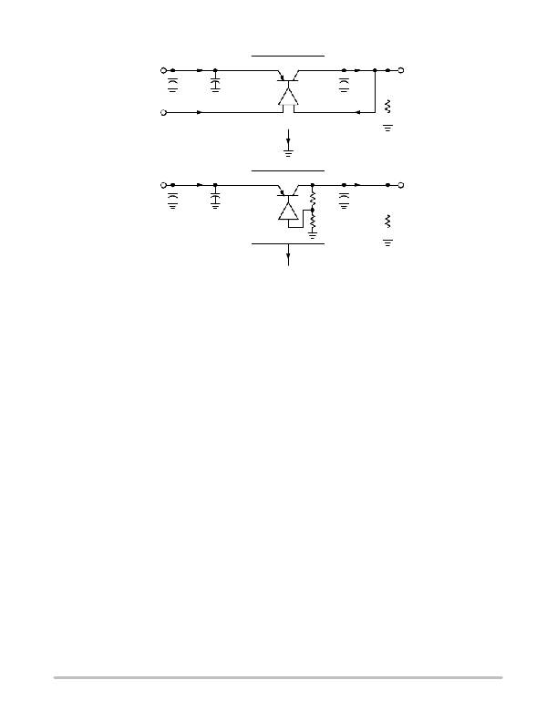
�NCP5500,� NCV5500,� NCP5501,� NCV5501�
�NCP5500�
�NCV5500�
�Input�
�I� in�
�V� in�
�V� out�
�I� out�
�Output�
�C� in�
�10� m� F�
�C� in2�
�100� nF�
�C� out�
�Enable�
�I� EN�
�EN�
�GND�
�ADJ�
�I� ADJ�
�R� L�
�I� GND�
�I� Q�
�NCP5501�
�NCV5501�
�Input�
�I� in�
�V� in�
�V� out�
�I� out�
�Output�
�C� in�
�10� m� F�
�C� in2�
�100� nF�
�C� out�
�R� L�
�GND�
�I� GND�
�I� Q�
�Figure� 21.� Measuring� Circuits�
�Circuit� Description�
�The� NCP5500/NCP5501/NCV5500/NCV5501� are�
�integrated� linear� regulators� with� a� DC� load� current�
�capability� of� 500� mA.� The� output� voltage� is� regulated� by� a�
�PNP� pass� transistor� controlled� by� an� error� amplifier� and�
�band� gap� reference.� The� choice� of� a� PNP� pass� element�
�provides� the� lowest� possible� dropout� voltage,� particularly� at�
�reduced� load� currents.� Pass� transistor� base� drive� current� is�
�controlled� to� prevent� oversaturation.� The� regulator� is�
�internally� protected� by� both� current� limit� and� thermal�
�shutdown.� Thermal� shutdown� occurs� when� the� junction�
�temperature� exceeds� 150� ?� C.� The� NCV5500� includes� an�
�enable/shutdown� pin� to� turn� off� the� regulator� to� a� low� current�
�drain� standby� state.�
�Regulator�
�The� error� amplifier� compares� the� reference� voltage� to� a�
�sample� of� the� output� voltage� (V� out� )� and� drives� the� base� of� a�
�PNP� series� pass� transistor� via� a� buffer.� The� reference� is� a�
�bandgap� design� for� enhanced� temperature� stability.�
�Saturation� control� of� the� PNP� pass� transistor� is� a� function� of�
�the� load� current� and� input� voltage.� Oversaturation� of� the�
�output� power� device� is� prevented,� and� quiescent� current� in�
�the� ground� pin� is� minimized.�
�Regulator� Stability� Considerations�
�The� input� capacitor� is� necessary� to� stabilize� the� input�
�impedance� to� reduce� transient� line� influences.� The� output�
�linear� regulator:� startup� delay,� load� transient� response� and�
�loop� stability.� The� capacitor� value� and� type� should� be� based�
�on� cost,� availability,� size� and� temperature� constraints.� Refer�
�to� Typical� Operating� Characteristics� for� stability� regions.�
�Enable� Input� (NCP5500,� NCV5500)�
�The� enable� pin� is� used� to� turn� the� regulator� on� or� off.� By�
�holding� the� pin� at� a� voltage� less� than� 0.4� V,� the� output� of� the�
�regulator� will� be� turned� off� to� a� minimal� current� drain� state.�
�When� the� voltage� at� the� Enable� pin� is� greater� than� 2.0� V,� the�
�output� of� the� regulator� will� be� enabled� and� rise� to� the�
�regulated� output� voltage.� The� Enable� pin� may� be� connected�
�directly� to� the� input� pin� to� provide� a� constant� enable� to� the�
�regulator.�
�Active� Load� Protection� in� Shutdown� (NCP5500,�
�NCV5500)�
�When� a� linear� regulator� is� disabled� (shutdown),� the� output�
�(load)� voltage� should� be� zero.� However,� stray� PC� board�
�leakage� paths,� output� capacitor� dielectric� absorption,� and�
�inductively� coupled� power� sources� can� cause� an� undesirable�
�regulator� output� voltage� if� load� current� is� low� or� zero.� The�
�NCV5500� features� a� load� protection� network� that� is� active�
�only� during� Shutdown� mode.� This� network� switches� in� a�
�shunt� current� path� (~500� m� A)� from� V� out� to� Ground.� This�
�feature� also� provides� a� controlled� (“soft”)� discharge� path� for�
�the� output� capacitor� after� a� transition� from� Enable� to�
�Shutdown.�
�capacitor� helps� determine� three� main� characteristics� of� a�
�http://onsemi.com�
�8�
�相关PDF资料 |
PDF描述 |
|---|---|
| IDT71V3559SA80BQGI | IC SRAM 4MBIT 80NS 165FBGA |
| S270K33SL0R64K7R | CAP CER 27PF 3KV 10% RADIAL |
| NCV5500DT50RKG | IC REG LDO 5V .5A DPAK-5 |
| HR-AAAUF8 | BATT PACK 9.6V AAA 650MAH NIMH |
| IDT71V3559SA80BQG8 | IC SRAM 4MBIT 80NS 165FBGA |
相关代理商/技术参数 |
参数描述 |
|---|---|
| NCV5501 | 制造商:ONSEMI 制造商全称:ON Semiconductor 功能描述:500 mA Linear Regulator |
| NCV5501DT15G | 功能描述:低压差稳压器 - LDO ANA LDO REG RoHS:否 制造商:Texas Instruments 最大输入电压:36 V 输出电压:1.4 V to 20.5 V 回动电压(最大值):307 mV 输出电流:1 A 负载调节:0.3 % 输出端数量: 输出类型:Fixed 最大工作温度:+ 125 C 安装风格:SMD/SMT 封装 / 箱体:VQFN-20 |
| NCV5501DT15RKG | 功能描述:低压差稳压器 - LDO ANA LDO REG RoHS:否 制造商:Texas Instruments 最大输入电压:36 V 输出电压:1.4 V to 20.5 V 回动电压(最大值):307 mV 输出电流:1 A 负载调节:0.3 % 输出端数量: 输出类型:Fixed 最大工作温度:+ 125 C 安装风格:SMD/SMT 封装 / 箱体:VQFN-20 |
| NCV5501DT33G | 功能描述:低压差稳压器 - LDO 500 mA 3.3V LDO RoHS:否 制造商:Texas Instruments 最大输入电压:36 V 输出电压:1.4 V to 20.5 V 回动电压(最大值):307 mV 输出电流:1 A 负载调节:0.3 % 输出端数量: 输出类型:Fixed 最大工作温度:+ 125 C 安装风格:SMD/SMT 封装 / 箱体:VQFN-20 |
| NCV5501DT33RKG | 功能描述:低压差稳压器 - LDO 500 mA 3.3V LDO RoHS:否 制造商:Texas Instruments 最大输入电压:36 V 输出电压:1.4 V to 20.5 V 回动电压(最大值):307 mV 输出电流:1 A 负载调节:0.3 % 输出端数量: 输出类型:Fixed 最大工作温度:+ 125 C 安装风格:SMD/SMT 封装 / 箱体:VQFN-20 |
发布紧急采购,3分钟左右您将得到回复。