参数资料
| 型号: | NCV7340D13R2G |
| 厂商: | ON Semiconductor |
| 文件页数: | 1/12页 |
| 文件大小: | 0K |
| 描述: | IC TXRX CAN HS LP 8SOIC |
| 标准包装: | 3,000 |
| 系列: | * |
Semiconductor Components Industries, LLC, 2014
March, 2014 Rev. 7
1
Publication Order Number:
NCV7340/D
NCV7340
High Speed Low Power CAN
Transceiver
Description
The NCV7340 CAN transceiver is the interface between a
controller area network (CAN) protocol controller and the physical
bus and may be used in both 12 V and 24 V systems. The transceiver
provides differential transmit capability to the bus and differential
receive capability to the CAN controller.
The NCV7340 is a new addition to the CAN highspeed transceiver
family and is an improved dropin replacement for the AMIS42665.
Due to the wide commonmode voltage range of the receiver inputs,
the NCV7340 is able to reach outstanding levels of electromagnetic
susceptibility (EMS). Similarly, extremely low electromagnetic
emission (EME) is achieved by the excellent matching of the output
signals.
Features
Compatible with the ISO 11898 Standard (ISO 118982, ISO
118985 and SAE J2284)
Low Quiescent Current
High Speed (up to 1 Mbps)
Ideally Suited for 12 V and 24 V Industrial and Automotive
Applications
Extremely Low Current Standby Mode with Wakeup via the Bus
Low EME CommonMode Choke is No Longer Required
Voltage Source via VSPLIT Pin for Stabilizing the Recessive Bus
Level (Further EMC Improvement)
No Disturbance of the Bus Lines with an Unpowered Node
Transmit Data (TxD) Dominant Timeout Function
Thermal Protection
Bus Pins Protected Against Transients in an Automotive
Environment
Bus and VSPLIT Pins ShortCircuit Proof to Supply Voltage and
Ground
Logic Level Inputs Compatible with 3.3 V Devices
Up to 110 Nodes can be Connected to the Same Bus in Function of
Topology
NCV Prefix for Automotive and Other Applications Requiring
Unique Site and Control Change Requirements; AECQ100
Qualified and PPAP Capable
These are PbFree Devices
Typical Applications
Automotive
Industrial Networks
http://onsemi.com
See detailed ordering and shipping information in the package
dimensions section on page 9 of this data sheet.
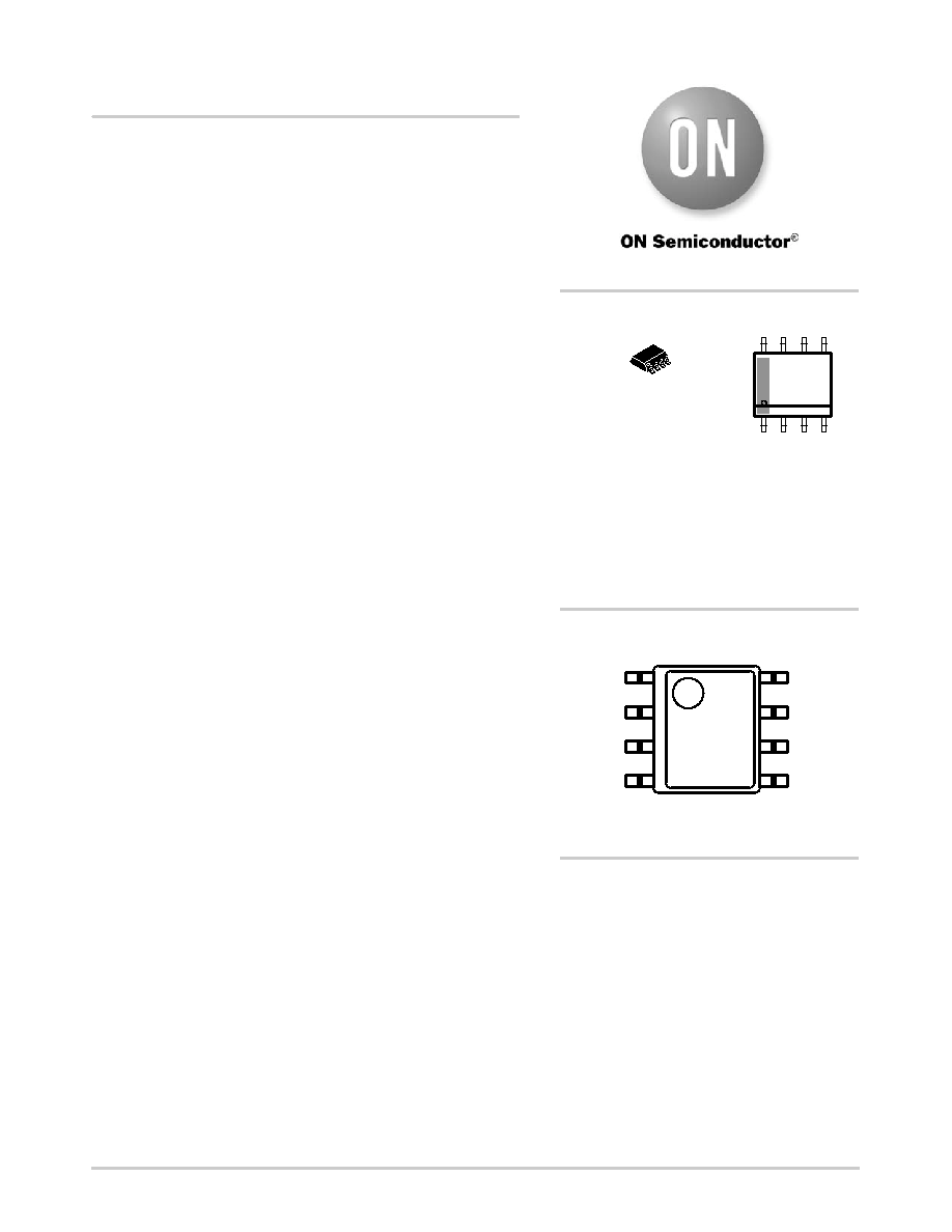
ORDERING INFORMATION
1
8
SOIC8
CASE 751AZ
PIN ASSIGNMENT
NV7340
= Specific Device Code
x
= 3 (NCV7340D13R2G)
= 2 (NCV7340D12R2G)
= 4 (NCV7340D14R2G)
A
= Assembly Location
L
= Wafer Lot
Y
= Year
W
= Work Week
G
= PbFree Package
NV7340x
ALYW
G
1
8
MARKING
DIAGRAM
NCV7340DxxR2G
(Top View)
5
6
7
8
1
2
3
4
TxD
RxD
STB
GND
CANL
VCC
VSPLIT
CANH
NCV7340
相关PDF资料 |
PDF描述 |
|---|---|
| MS27497T12F35PB | CONN RCPT 22POS WALL MNT W/PINS |
| NCV7340D12R2G | IC HS CAN TRANSC 8SOIC |
| MAX111BCWE+T | IC ADC 14BIT 2CH 16-SOIC |
| IDT72285L20TFI8 | IC FIFO 65536X18 LP 20NS 64STQFP |
| MS27497T12B35PC | CONN RCPT 22POS WALL MNT W/PINS |
相关代理商/技术参数 |
参数描述 |
|---|---|
| NCV7340D14G | 功能描述:CAN 接口集成电路 HS CAN TRANSC. (EDGE-WU) RoHS:否 制造商:Texas Instruments 类型:Transceivers 工作电源电压:5 V 电源电流: 工作温度范围:- 40 C to + 85 C 封装 / 箱体:SOIC-8 封装:Tube |
| NCV7340D14R2G | 功能描述:CAN 接口集成电路 HS CAN TRANSC. (EDGE-WU) RoHS:否 制造商:Texas Instruments 类型:Transceivers 工作电源电压:5 V 电源电流: 工作温度范围:- 40 C to + 85 C 封装 / 箱体:SOIC-8 封装:Tube |
| NCV7341 | 制造商:ONSEMI 制造商全称:ON Semiconductor 功能描述:High Speed Low Power CAN Transceiver |
| NCV7341D20G | 功能描述:CAN 接口集成电路 IMPR. HS LP CAN TRANSC. + RoHS:否 制造商:Texas Instruments 类型:Transceivers 工作电源电压:5 V 电源电流: 工作温度范围:- 40 C to + 85 C 封装 / 箱体:SOIC-8 封装:Tube |
| NCV7341D20R2G | 功能描述:CAN 接口集成电路 IMPR. HS LP CAN TRANSC. + RoHS:否 制造商:Texas Instruments 类型:Transceivers 工作电源电压:5 V 电源电流: 工作温度范围:- 40 C to + 85 C 封装 / 箱体:SOIC-8 封装:Tube |
发布紧急采购,3分钟左右您将得到回复。