参数资料
| 型号: | NCV8570BMN300R2G |
| 厂商: | ON Semiconductor |
| 文件页数: | 2/20页 |
| 文件大小: | 0K |
| 描述: | IC REG LDO 3V .2A 6DFN |
| 标准包装: | 1 |
| 稳压器拓扑结构: | 正,固定式 |
| 输出电压: | 3V |
| 输入电压: | 最高 5.5V |
| 电压 - 压降(标准): | 0.115V @ 200mA |
| 稳压器数量: | 1 |
| 电流 - 输出: | 200mA |
| 电流 - 限制(最小): | 200mA |
| 工作温度: | -40°C ~ 125°C |
| 安装类型: | 表面贴装 |
| 封装/外壳: | 6-VDFN 裸露焊盘 |
| 供应商设备封装: | 6-DFN(2x2.2) |
| 包装: | 标准包装 |
| 其它名称: | NCV8570BMN300R2GOSDKR |
��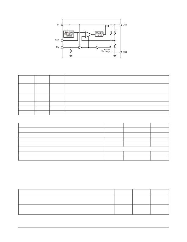 �
�
�NCV8570B�
�R� DIS�
�R� PD�
�Figure� 2.� Simplified� Block� Diagram�
�PIN� FUNCTION� DESCRIPTION�
�Pin� No.�
�Pin� No.�
�DFN6�
�1�
�2,� 5,� EPAD�
�3�
�4�
�6�
�TSOP� ?� 5�
�3�
�2�
�1�
�5�
�4�
�Pin� Name�
�EN�
�GND�
�IN�
�OUT�
�BYP�
�Description�
�Enable� pin:� This� pin� allows� on/off� control� of� the� regulator.� To� disable� the� device,� connect� to�
�GND.� If� this� function� is� not� in� use,� connect� to� Vin.� Internal� 5� M� W� Pull� Down� resistor� is�
�connected� between� EN� and� GND.�
�Power� Supply� Ground� (Pins� are� fused� for� the� DFN6� package).� Pins� 2,� 5� and� EPAD� are�
�connected� together� through� the� lead� frame� in� the� DFN6� package.�
�Power� Supply� Input� Voltage�
�Regulated� Output� Voltage�
�Noise� reduction� pin.� (Connect� 10� nF� or� 100� nF� capacitor� to� GND)�
�MAXIMUM� RATINGS�
�Input� Voltage� (Note� 2)�
�Chip� Enable� Voltage�
�Noise� Reduction� Voltage�
�Output� Voltage�
�Output� Short� ?� Circuit� Duration�
�Maximum� Junction� Temperature�
�Storage� Temperature� Range�
�Rating�
�Symbol�
�IN�
�EN�
�BYP�
�OUT�
�T� J(max)�
�T� STG�
�Value�
�?� 0.3� V� to� 6� V�
�?� 0.3� V� to� V� IN� +0.3� V�
�?� 0.3� V� to� V� IN� +0.3� V�
�?� 0.3� V� to� V� IN� +0.3� V�
�Infinity�
�125�
�?� 55� to� 150�
�Unit�
�V�
�V�
�V�
�?� C�
�?� C�
�Stresses� exceeding� Maximum� Ratings� may� damage� the� device.� Maximum� Ratings� are� stress� ratings� only.� Functional� operation� above� the�
�Recommended� Operating� Conditions� is� not� implied.� Extended� exposure� to� stresses� above� the� Recommended� Operating� Conditions� may�
�affect� device� reliability.�
�1.� This� device� series� contains� ESD� protection� and� exceeds� the� following� tests:�
�Human� Body� Model� 2000� V� tested� per� MIL� ?� STD� ?� 883,� Method� 3015�
�Machine� Model� Method� 200� V�
�This� device� meets� or� exceeds� AEC� ?� Q100� standard.�
�THERMAL� CHARACTERISTICS�
�Rating�
�Package� Thermal� Resistance,� DFN6:� (Notes� 2,� 3)�
�Junction� ?� to� ?� Case� (Pin� 2)�
�Junction� ?� to� ?� Ambient�
�Package� Thermal� Resistance,� TSOP� ?� 5:� (Notes� 2,� 3)�
�Junction� ?� to� ?� Case� (Pin� 2)�
�Junction� ?� to� ?� Ambient�
�Symbol�
�Y� JL2�
�R� q� JA�
�Y� JL2�
�R� q� JA�
�Value�
�38�
�110�
�92�
�204�
�Unit�
�?� C� /W�
�?� C� /W�
�2.� Refer� to� APPLICATION� INFORMATION� for� Safe� Operating� Area�
�3.� Single� component� mounted� on� 1� oz,� FR4� PCB� with� 645mm� 2� Cu� area.�
�http://onsemi.com�
�2�
�相关PDF资料 |
PDF描述 |
|---|---|
| NCV8570BSN25T1G | IC REG LDO 2.5V .2A 5TSOP |
| NCV8570MN330R2G | IC REG LDO 3.3V .2A 6-DFN |
| NCV8603SN33T1G | IC REG LDO 3.3V .3A 5TSOP |
| NCV8612BMNR2G | IC REG LDO 5V/3.3V/ADJ 20DFN |
| NCV8612MNR2G | IC REG LDO 5V/3.3V/ADJ 20DFN |
相关代理商/技术参数 |
参数描述 |
|---|---|
| NCV8570BMN330R2G | 功能描述:低压差稳压器 - LDO 200MA ULN RF LDO REG3.3V RoHS:否 制造商:Texas Instruments 最大输入电压:36 V 输出电压:1.4 V to 20.5 V 回动电压(最大值):307 mV 输出电流:1 A 负载调节:0.3 % 输出端数量: 输出类型:Fixed 最大工作温度:+ 125 C 安装风格:SMD/SMT 封装 / 箱体:VQFN-20 |
| NCV8570BSN18T1G | 功能描述:低压差稳压器 - LDO 200MA ULN RF LDO REG1.8V RoHS:否 制造商:Texas Instruments 最大输入电压:36 V 输出电压:1.4 V to 20.5 V 回动电压(最大值):307 mV 输出电流:1 A 负载调节:0.3 % 输出端数量: 输出类型:Fixed 最大工作温度:+ 125 C 安装风格:SMD/SMT 封装 / 箱体:VQFN-20 |
| NCV8570BSN25T1G | 功能描述:低压差稳压器 - LDO 200MA ULN RF LDO REG2.5V RoHS:否 制造商:Texas Instruments 最大输入电压:36 V 输出电压:1.4 V to 20.5 V 回动电压(最大值):307 mV 输出电流:1 A 负载调节:0.3 % 输出端数量: 输出类型:Fixed 最大工作温度:+ 125 C 安装风格:SMD/SMT 封装 / 箱体:VQFN-20 |
| NCV8570BSN28T1G | 功能描述:低压差稳压器 - LDO 200MA ULN RF LDO REG2.8V RoHS:否 制造商:Texas Instruments 最大输入电压:36 V 输出电压:1.4 V to 20.5 V 回动电压(最大值):307 mV 输出电流:1 A 负载调节:0.3 % 输出端数量: 输出类型:Fixed 最大工作温度:+ 125 C 安装风格:SMD/SMT 封装 / 箱体:VQFN-20 |
| NCV8570BSN30T1G | 功能描述:低压差稳压器 - LDO 200MA ULN RF LDO REG 3V RoHS:否 制造商:Texas Instruments 最大输入电压:36 V 输出电压:1.4 V to 20.5 V 回动电压(最大值):307 mV 输出电流:1 A 负载调节:0.3 % 输出端数量: 输出类型:Fixed 最大工作温度:+ 125 C 安装风格:SMD/SMT 封装 / 箱体:VQFN-20 |
发布紧急采购,3分钟左右您将得到回复。