- 您现在的位置:买卖IC网 > PDF目录13686 > NCV8842MNR2G (ON Semiconductor)IC REG BUCK 1.5A 18DFN PDF资料下载
参数资料
| 型号: | NCV8842MNR2G |
| 厂商: | ON Semiconductor |
| 文件页数: | 6/16页 |
| 文件大小: | 0K |
| 描述: | IC REG BUCK 1.5A 18DFN |
| 标准包装: | 1 |
| 类型: | 降压(降压) |
| 输出数: | 1 |
| 输入电压: | 4.5 V ~ 40 V |
| PWM 型: | 混合物 |
| 频率 - 开关: | 170kHz |
| 电流 - 输出: | 1.5A |
| 同步整流器: | 无 |
| 工作温度: | -40°C ~ 150°C |
| 安装类型: | 表面贴装 |
| 封装/外壳: | 18-VFDFN 裸露焊盘 |
| 包装: | 剪切带 (CT) |
| 供应商设备封装: | 18-DFN(5x6) |
| 其它名称: | NCV8842MNR2GOSCT |
�� �
�
�NCV8842�
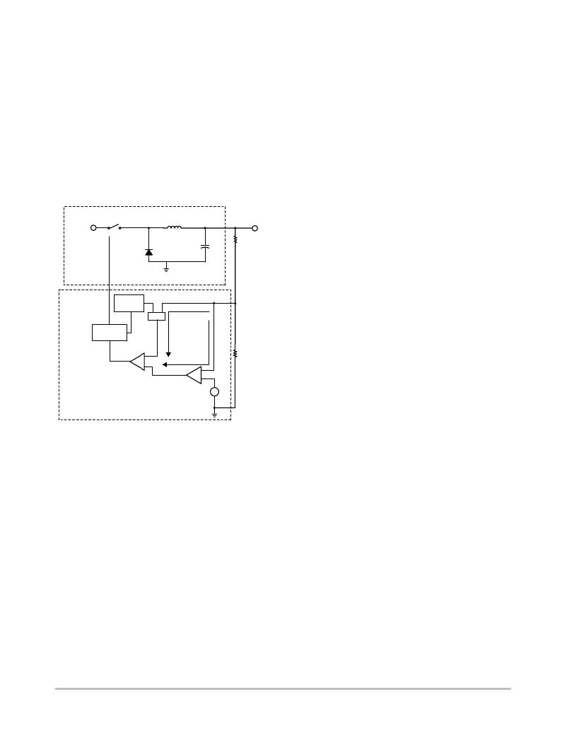
�APPLICATIONS� INFORMATION�
�THEORY� OF� OPERATION�
�V� 2� Control�
�The� NCV8842� buck� regulator� provides� a� high� level� of�
�integration� and� high� operating� frequencies� allowing� the�
�layout� of� a� switch� ?� mode� power� supply� in� a� very� small� board�
�area.� This� device� is� based� on� the� proprietary� V� 2� control�
�architecture.� V� 2� control� uses� the� output� voltage� and� its� ripple�
�as� the� ramp� signal,� providing� an� ease� of� use� not� generally�
�associated� with� voltage� or� current� mode� control.� Improved�
�line� regulation,� load� regulation� and� very� fast� transient�
�response� are� also� major� advantages.�
�current� of� the� inductor� L1� and� the� ESR� (equivalent� series�
�resistor)� of� the� output� capacitor� C1.�
�The� slope� compensation� signal� is� a� fixed� voltage� ramp�
�provided� by� the� oscillator.� Adding� this� signal� eliminates�
�subharmonic� oscillation� associated� with� the� operation� at�
�duty� cycle� greater� than� 50%.� The� artificial� ramp� also� ensures�
�the� proper� PWM� function� when� the� output� ripple� voltage� is�
�inadequate.� The� slope� compensation� signal� is� properly� sized�
�to� serve� it� purposes� without� sacrificing� the� transient�
�response� speed.�
�Under� load� and� line� transient,� not� only� the� ramp� signal�
�changes,� but� more� significantly� the� DC� component� of� the�
�feedback� voltage� varies� proportionally� to� the� output� voltage.�
�V� IN�
�Duty� Cycle�
�S1�
�D1�
�L1�
�C1�
�R1�
�V� O�
�FFB� path� connects� both� signals� directly� to� the� PWM�
�comparator.� This� allows� instant� modulation� of� the� duty� cycle�
�to� counteract� any� output� voltage� deviations.� The� transient�
�response� time� is� independent� of� the� error� amplifier�
�Buck�
�Controller�
�bandwidth.� This� eliminates� the� delay� associated� with� error�
�amplifier� and� greatly� improves� the� transient� response� time.�
�The� error� amplifier� is� used� here� to� ensure� excellent� DC�
�Latch� S�
�V� 2�
�Control�
�Oscillator�
�R�
�PWM� Com-�
�parator�
�Slope�
�Comp�
�FFB�
�SFB�
�V� C�
�Error�
�Amplifier�
�+�
�?�
�V� REF�
�V� FB�
�R2�
�accuracy.�
�Error� Amplifier�
�The� NCV8842� has� a� transconductance� error� amplifier,�
�whose� non� ?� inverting� input� is� connected� to� an� Internal�
�Reference� Voltage� generated� from� the� on� ?� chip� regulator.�
�The� inverting� input� connects� to� the� V� FB� pin.� The� output� of�
�the� error� amplifier� is� made� available� at� the� V� C� pin.� A� typical�
�frequency� compensation� requires� only� a� 0.1� m� F� capacitor�
�connected� between� the� V� C� pin� and� ground,� as� shown� in�
�Figure� 1.� This� capacitor� and� error� amplifier� ’s� output�
�resistance� (approximately� 8.0� M� W� )� create� a� low� frequency�
�pole� to� limit� the� bandwidth.� Since� V� 2� control� does� not�
�Figure� 3.� Buck� Converter� with� V� 2� Control.�
�As� shown� in� Figure� 3,� there� are� two� voltage� feedback�
�paths� in� V� 2� control,� namely� FFB(Fast� Feedback)� and�
�SFB(Slow� Feedback).� In� FFB� path,� the� feedback� voltage�
�connects� directly� to� the� PWM� comparator.� This� feedback�
�path� carries� the� ramp� signal� as� well� as� the� output� DC� voltage.�
�Artificial� ramp� derived� from� the� oscillator� is� added� to� the�
�feedback� signal� to� improve� stability.� The� other� feedback�
�path,� SFB,� connects� the� feedback� voltage� to� the� error�
�amplifier� whose� output� V� C� feeds� to� the� other� input� of� the�
�PWM� comparator.� In� a� constant� frequency� mode,� the�
�oscillator� signal� sets� the� output� latch� and� turns� on� the� switch�
�S1.� This� starts� a� new� switch� cycle.� The� ramp� signal,�
�composed� of� both� artificial� ramp� and� output� ripple,�
�eventually� comes� across� the� V� C� voltage,� and� consequently�
�resets� the� latch� to� turn� off� the� switch.� The� switch� S1� will� turn�
�on� again� at� the� beginning� of� the� next� switch� cycle.� In� a� buck�
�converter,� the� output� ripple� is� determined� by� the� ripple�
�require� a� high� bandwidth� error� amplifier,� the� frequency�
�compensation� is� greatly� simplified.�
�The� V� C� pin� is� clamped� below� Output� High� Voltage.� This�
�allows� the� regulator� to� recover� quickly� from� over� current� or�
�short� circuit� conditions.�
�Oscillator� and� Sync� Feature�
�The� on� ?� chip� oscillator� is� trimmed� at� the� factory� and�
�requires� no� external� components� for� frequency� control.� The�
�high� switching� frequency� allows� smaller� external�
�components� to� be� used,� resulting� in� a� board� area� and� cost�
�savings.� The� tight� frequency� tolerance� simplifies� magnetic�
�components� selection.� The� switching� frequency� is� reduced�
�to� no� more� than� 25%� of� the� nominal� value� when� the� V� FB� pin�
�voltage� is� below� Frequency� Foldback� Threshold.� In� short�
�circuit� or� over� ?� load� conditions,� this� reduces� the� power�
�dissipation� of� the� IC� and� external� components.�
�The� oscillator� frequency� varies� with� junction�
�temperature,� as� seen� in� the� following� graph.�
�http://onsemi.com�
�6�
�相关PDF资料 |
PDF描述 |
|---|---|
| VE-2TP-EX-F4 | CONVERTER MOD DC/DC 13.8V 75W |
| VE-2TP-EX-F3 | CONVERTER MOD DC/DC 13.8V 75W |
| VE-2TP-EX-F2 | CONVERTER MOD DC/DC 13.8V 75W |
| GMM18DTMN | CONN EDGECARD 36POS R/A .156 SLD |
| VE-2TN-EX-F3 | CONVERTER MOD DC/DC 18.5V 75W |
相关代理商/技术参数 |
参数描述 |
|---|---|
| NCV8842MNR2GEVB | 功能描述:BOARD EVAL FOR NCV8842 RoHS:是 类别:编程器,开发系统 >> 评估板 - DC/DC 与 AC/DC(离线)SMPS 系列:- 产品培训模块:Obsolescence Mitigation Program 标准包装:1 系列:True Shutdown™ 主要目的:DC/DC,步升 输出及类型:1,非隔离 功率 - 输出:- 输出电压:- 电流 - 输出:1A 输入电压:2.5 V ~ 5.5 V 稳压器拓扑结构:升压 频率 - 开关:3MHz 板类型:完全填充 已供物品:板 已用 IC / 零件:MAX8969 |
| NCV8842PWG | 功能描述:直流/直流开关转换器 1.5A LO VLT BUCK REG RoHS:否 制造商:STMicroelectronics 最大输入电压:4.5 V 开关频率:1.5 MHz 输出电压:4.6 V 输出电流:250 mA 输出端数量:2 最大工作温度:+ 85 C 安装风格:SMD/SMT |
| NCV8842PWGEVB | 功能描述:电源管理IC开发工具 NCV8842 EVAL BRD RoHS:否 制造商:Maxim Integrated 产品:Evaluation Kits 类型:Battery Management 工具用于评估:MAX17710GB 输入电压: 输出电压:1.8 V |
| NCV8842PWR2G | 功能描述:直流/直流开关转换器 1.5A LO VLT BUCK REG RoHS:否 制造商:STMicroelectronics 最大输入电压:4.5 V 开关频率:1.5 MHz 输出电压:4.6 V 输出电流:250 mA 输出端数量:2 最大工作温度:+ 85 C 安装风格:SMD/SMT |
| NCV8843 | 制造商:ONSEMI 制造商全称:ON Semiconductor 功能描述:1.5 A, 340 kHz, Buck Regulator with Synchronization Capability |
发布紧急采购,3分钟左右您将得到回复。