- 您现在的位置:买卖IC网 > PDF目录13686 > NCV8842MNR2G (ON Semiconductor)IC REG BUCK 1.5A 18DFN PDF资料下载
参数资料
| 型号: | NCV8842MNR2G |
| 厂商: | ON Semiconductor |
| 文件页数: | 7/16页 |
| 文件大小: | 0K |
| 描述: | IC REG BUCK 1.5A 18DFN |
| 标准包装: | 1 |
| 类型: | 降压(降压) |
| 输出数: | 1 |
| 输入电压: | 4.5 V ~ 40 V |
| PWM 型: | 混合物 |
| 频率 - 开关: | 170kHz |
| 电流 - 输出: | 1.5A |
| 同步整流器: | 无 |
| 工作温度: | -40°C ~ 150°C |
| 安装类型: | 表面贴装 |
| 封装/外壳: | 18-VFDFN 裸露焊盘 |
| 包装: | 剪切带 (CT) |
| 供应商设备封装: | 18-DFN(5x6) |
| 其它名称: | NCV8842MNR2GOSCT |
�� �
�
�NCV8842�
�102.5�
�100�
�97.5�
�95�
�92.5�
�90�
�?� 40� ?� 20� 0� 20� 40� 60� 80� 100� 120� 140�
�T� J� ,� JUNCTION� TEMPERATURE� (� °� C)�
�Figure� 4.� Oscillator� Frequency� Versus� Junction�
�Temperature�
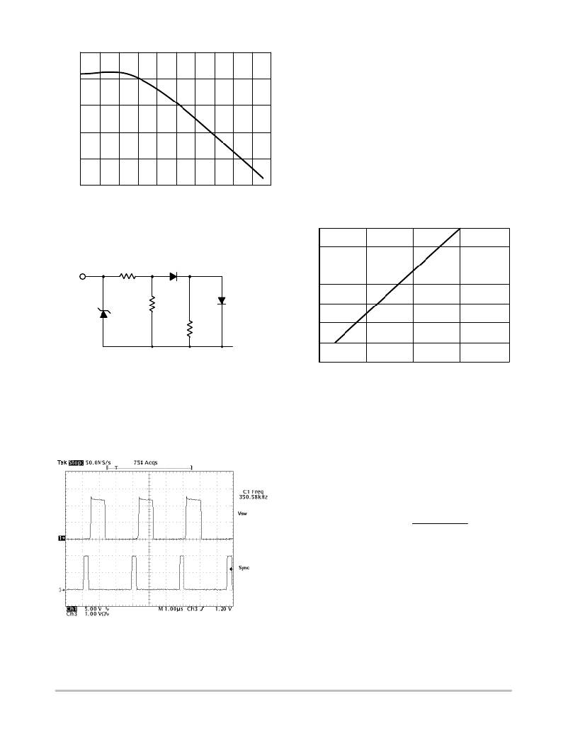
�An� external� clock� signal� can� sync� the� NCV8842� to� a�
�higher� frequency.� The� SYNC� pin� equivalent� input� circuit� is�
�shown� in� Figure� 5.�
�Power� Switch� and� Current� Limit�
�The� collector� of� the� built� ?� in� NPN� power� switch� is�
�connected� to� the� V� IN� pin,� and� the� emitter� to� the� V� SW� pin.�
�When� the� switch� turns� on,� the� V� SW� voltage� is� equal� to� the�
�V� IN� minus� switch� Saturation� Voltage.� In� the� buck� regulator,�
�the� V� SW� voltage� swings� to� one� diode� drop� below� ground�
�when� the� power� switch� turns� off,� and� the� inductor� current� is�
�commutated� to� the� catch� diode.� Due� to� the� presence� of� high�
�pulsed� current,� the� traces� connecting� the� V� SW� pin,� inductor�
�and� diode� should� be� kept� as� short� as� possible� to� minimize� the�
�noise� and� radiation.� For� the� same� reason,� the� input� capacitor�
�should� be� placed� close� to� the� V� IN� pin� and� the� anode� of� the�
�diode.�
�The� saturation� voltage� of� the� power� switch� is� dependent�
�on� the� switching� current,� as� shown� in� Figure� 7.�
�1.0�
�0.9�
�0.8�
�Sync�
�10k�
�±� 33%�
�V� Z� =� 11V�
�to� 20V�
�50k�
�±� 33%�
�50k�
�±� 33%�
�0.7�
�0.6�
�0.5�
�IO(MAX)� +� ILIM� *� O�
�GND�
�Figure� 5.�
�The� rising� edge� of� the� sync� pulse� turns� on� the� power�
�switch� to� start� a� new� switching� cycle,� as� shown� in� Figure� 6.�
�There� is� approximately� 0.5� m� s� delay� between� the� rising� edge�
�of� the� sync� pulse� and� rising� edge� of� the� V� SW� pin� voltage.� The�
�sync� threshold� is� TTL� logic� compatible,� and� duty� cycle� of�
�the� sync� pulses� can� vary� from� 10%� to� 90%.� The� frequency�
�foldback� feature� is� disabled� during� the� sync� mode.�
�Figure� 6.� A� NCV8842� Buck� Regulator� is� Synchronized�
�to� an� External� 350� kHz� Pulse� Signal�
�0.4�
�0.3�
�0� 0.5� 1.0� 1.5� 2.0�
�SWITCHING� CURRENT� (A)�
�Figure� 7.� Power� Switch� Saturation� Versus� Switching�
�Current� (Normalized� to� 1.5� A)�
�The� NCV8842� contains� pulse� ?� by� ?� pulse� current� limiting�
�to� protect� the� power� switch� and� external� components.� When�
�the� peak� of� the� switching� current� reaches� the� Current� Limit,�
�the� power� switch� turns� off� after� the� Current� Limit� Delay.� The�
�switch� will� not� turn� on� until� the� next� switching� cycle.� The�
�current� limit� threshold� is� independent� of� switching� duty�
�cycle.� The� maximum� load� current,� given� by� the� following�
�formula� under� continuous� conduction� mode,� is� less� than� the�
�Current� Limit� due� to� the� ripple� current.�
�V (VIN� *� VO)�
�2(L)(VIN)(fs)�
�where:�
�f� S� =� switching� frequency,�
�I� LIM� =� current� limit� threshold,�
�V� O� =� output� voltage,�
�V� IN� =� input� voltage,�
�L� =� inductor� value.�
�When� the� regulator� runs� under� current� limit,� the�
�subharmonic� oscillation� may� cause� low� frequency�
�http://onsemi.com�
�7�
�相关PDF资料 |
PDF描述 |
|---|---|
| VE-2TP-EX-F4 | CONVERTER MOD DC/DC 13.8V 75W |
| VE-2TP-EX-F3 | CONVERTER MOD DC/DC 13.8V 75W |
| VE-2TP-EX-F2 | CONVERTER MOD DC/DC 13.8V 75W |
| GMM18DTMN | CONN EDGECARD 36POS R/A .156 SLD |
| VE-2TN-EX-F3 | CONVERTER MOD DC/DC 18.5V 75W |
相关代理商/技术参数 |
参数描述 |
|---|---|
| NCV8842MNR2GEVB | 功能描述:BOARD EVAL FOR NCV8842 RoHS:是 类别:编程器,开发系统 >> 评估板 - DC/DC 与 AC/DC(离线)SMPS 系列:- 产品培训模块:Obsolescence Mitigation Program 标准包装:1 系列:True Shutdown™ 主要目的:DC/DC,步升 输出及类型:1,非隔离 功率 - 输出:- 输出电压:- 电流 - 输出:1A 输入电压:2.5 V ~ 5.5 V 稳压器拓扑结构:升压 频率 - 开关:3MHz 板类型:完全填充 已供物品:板 已用 IC / 零件:MAX8969 |
| NCV8842PWG | 功能描述:直流/直流开关转换器 1.5A LO VLT BUCK REG RoHS:否 制造商:STMicroelectronics 最大输入电压:4.5 V 开关频率:1.5 MHz 输出电压:4.6 V 输出电流:250 mA 输出端数量:2 最大工作温度:+ 85 C 安装风格:SMD/SMT |
| NCV8842PWGEVB | 功能描述:电源管理IC开发工具 NCV8842 EVAL BRD RoHS:否 制造商:Maxim Integrated 产品:Evaluation Kits 类型:Battery Management 工具用于评估:MAX17710GB 输入电压: 输出电压:1.8 V |
| NCV8842PWR2G | 功能描述:直流/直流开关转换器 1.5A LO VLT BUCK REG RoHS:否 制造商:STMicroelectronics 最大输入电压:4.5 V 开关频率:1.5 MHz 输出电压:4.6 V 输出电流:250 mA 输出端数量:2 最大工作温度:+ 85 C 安装风格:SMD/SMT |
| NCV8843 | 制造商:ONSEMI 制造商全称:ON Semiconductor 功能描述:1.5 A, 340 kHz, Buck Regulator with Synchronization Capability |
发布紧急采购,3分钟左右您将得到回复。