- 您现在的位置:买卖IC网 > PDF目录17277 > NID9N05CL (ON Semiconductor)MOSFET N-CH CLAMP 9A 52V DPAK PDF资料下载
参数资料
| 型号: | NID9N05CL |
| 厂商: | ON Semiconductor |
| 文件页数: | 6/7页 |
| 文件大小: | 0K |
| 描述: | MOSFET N-CH CLAMP 9A 52V DPAK |
| 产品变化通告: | Product Discontinuation 09/Jan/2008 |
| 标准包装: | 75 |
| 类型: | 低端 |
| 输入类型: | 非反相 |
| 输出数: | 1 |
| 导通状态电阻: | 153 毫欧 |
| 电流 - 峰值输出: | 9A |
| 工作温度: | -55°C ~ 175°C |
| 安装类型: | 表面贴装 |
| 封装/外壳: | TO-252-3,DPak(2 引线+接片),SC-63 |
| 供应商设备封装: | DPAK-3 |
| 包装: | 管件 |
�� �
�
�NID9N05CL,� NID9N05ACL�
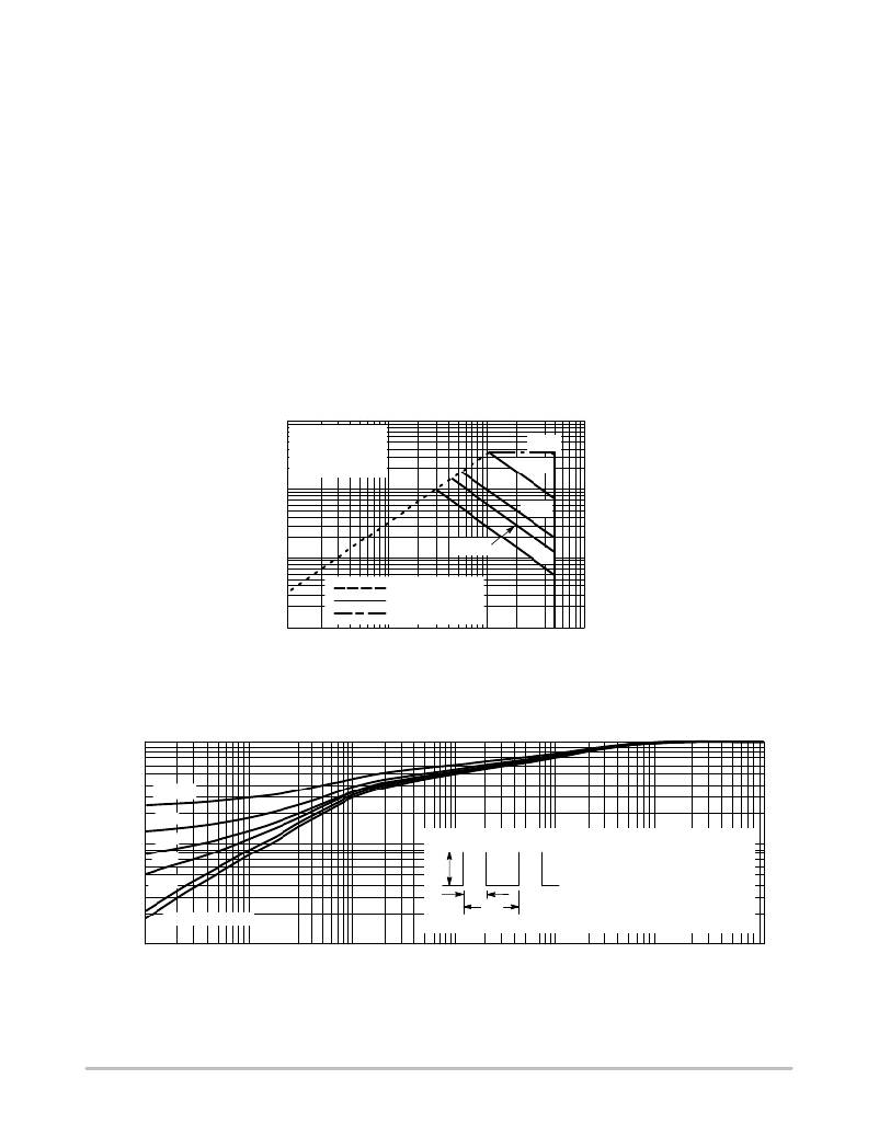
�SAFE� OPERATING� AREA�
�The� Forward� Biased� Safe� Operating� Area� curves� define�
�the� maximum� simultaneous� drain� ?� to� ?� source� voltage� and�
�drain� current� that� a� transistor� can� handle� safely� when� it� is�
�forward� biased.� Curves� are� based� upon� maximum� peak�
�junction� temperature� and� a� case� temperature� (T� C� )� of� 25� °� C.�
�Peak� repetitive� pulsed� power� limits� are� determined� by� using�
�the� thermal� response� data� in� conjunction� with� the� procedures�
�discussed� in� AN569,� “Transient� Thermal� Resistance� ?�
�General� Data� and� Its� Use.”�
�Switching� between� the� off� ?� state� and� the� on� ?� state� may�
�traverse� any� load� line� provided� neither� rated� peak� current�
�(I� DM� )� nor� rated� voltage� (V� DSS� )� is� exceeded� and� the�
�transition� time� (t� r� ,t� f� )� do� not� exceed� 10� m� s.� In� addition� the� total�
�power� averaged� over� a� complete� switching� cycle� must� not�
�exceed� (T� J(MAX)� ?� T� C� )/(R� q� JC� ).�
�A� Power� MOSFET� designated� E� ?� FET� can� be� safely� used�
�in� switching� circuits� with� unclamped� inductive� loads.� For�
�100�
�V� GS� =� 12� V�
�SINGLE� PULSE�
�T� C� =� 25� °� C�
�reliable� operation,� the� stored� energy� from� circuit� inductance�
�dissipated� in� the� transistor� while� in� avalanche� must� be� less�
�than� the� rated� limit� and� adjusted� for� operating� conditions�
�differing� from� those� specified.� Although� industry� practice� is�
�to� rate� in� terms� of� energy,� avalanche� energy� capability� is� not�
�a� constant.� The� energy� rating� decreases� non� ?� linearly� with� an�
�increase� of� peak� current� in� avalanche� and� peak� junction�
�temperature.�
�Although� many� E� ?� FETs� can� withstand� the� stress� of�
�drain� ?� to� ?� source� avalanche� at� currents� up� to� rated� pulsed�
�current� (I� DM� ),� the� energy� rating� is� specified� at� rated�
�continuous� current� (I� D� ),� in� accordance� with� industry� custom.�
�The� energy� rating� must� be� derated� for� temperature� as� shown�
�in� the� accompanying� graph� (Figure� 12).� Maximum� energy� at�
�currents� below� rated� continuous� I� D� can� safely� be� assumed� to�
�equal� the� values� indicated.�
�10� m� s�
�100� m� s�
�10�
�1� ms�
�1�
�10 ms�
�R� DS(on)� LIMIT�
�THERMAL� LIMIT�
�dc�
�0.1�
�0.1�
�PACKAGE� LIMIT�
�1�
�10�
�100�
�V� DS� ,� DRAIN� ?� TO� ?� SOURCE� VOLTAGE� (VOLTS)�
�Figure� 11.� Maximum� Rated� Forward� Biased�
�Safe� Operating� Area�
�1.0�
�D = 0.5�
�0.2�
�0.1�
�0.1�
�0.05�
�0.01�
�SINGLE PULSE�
�P� (pk)�
�t� 1�
�t� 2�
�DUTY� CYCLE,� D� =� t� 1� /t� 2�
�R� q� JC� (t)� =� r(t)� R� q� JC�
�D� CURVES� APPLY� FOR� POWER�
�PULSE� TRAIN� SHOWN�
�READ� TIME� AT� t� 1�
�T� J(pk)� ?� T� C� =� P� (pk)� R� q� JC� (t)�
�0.01�
�0.00001�
�0.0001�
�0.001�
�0.01�
�0.1�
�1�
�10�
�t,� TIME� (s)�
�Figure� 12.� Thermal� Response�
�http://onsemi.com�
�6�
�相关PDF资料 |
PDF描述 |
|---|---|
| RMM06DTKN | CONN EDGECARD 12POS DIP .156 SLD |
| 591D477X0004C2T20H | CAP TANT 470UF 4V 20% 2812 |
| 591D476X9016C2T20H | CAP TANT 47UF 16V 10% 2812 |
| 591D476X0016C2T20H | CAP TANT 47UF 16V 20% 2812 |
| 050R30-102B | CABLE FLAT FLEX 30POS 0.5MM 4" |
相关代理商/技术参数 |
参数描述 |
|---|---|
| NID9N05CL_06 | 制造商:ONSEMI 制造商全称:ON Semiconductor 功能描述:Power MOSFET |
| NID9N05CLG | 功能描述:MOSFET 52V 9A N-Channel RoHS:否 制造商:STMicroelectronics 晶体管极性:N-Channel 汲极/源极击穿电压:650 V 闸/源击穿电压:25 V 漏极连续电流:130 A 电阻汲极/源极 RDS(导通):0.014 Ohms 配置:Single 最大工作温度: 安装风格:Through Hole 封装 / 箱体:Max247 封装:Tube |
| NID9N05CLT4 | 功能描述:MOSFET 52V 9A N-Channel RoHS:否 制造商:STMicroelectronics 晶体管极性:N-Channel 汲极/源极击穿电压:650 V 闸/源击穿电压:25 V 漏极连续电流:130 A 电阻汲极/源极 RDS(导通):0.014 Ohms 配置:Single 最大工作温度: 安装风格:Through Hole 封装 / 箱体:Max247 封装:Tube |
| NID9N05CLT4G | 功能描述:MOSFET 52V 9A N-Channel RoHS:否 制造商:STMicroelectronics 晶体管极性:N-Channel 汲极/源极击穿电压:650 V 闸/源击穿电压:25 V 漏极连续电流:130 A 电阻汲极/源极 RDS(导通):0.014 Ohms 配置:Single 最大工作温度: 安装风格:Through Hole 封装 / 箱体:Max247 封装:Tube |
| NIDAQCARD-6533 | 制造商:NI 制造商全称:National Instruments Corporation 功能描述:High-Speed 32-bit Digital Pattern I/O and Handshaking |
发布紧急采购,3分钟左右您将得到回复。