参数资料
| 型号: | NL27WZ125USG |
| 厂商: | ON Semiconductor |
| 文件页数: | 2/5页 |
| 文件大小: | 0K |
| 描述: | IC BUFFER DL TRI-ST NON-INV US8 |
| 标准包装: | 1 |
| 系列: | 27WZ |
| 逻辑类型: | 缓冲器/线路驱动器,非反相 |
| 元件数: | 2 |
| 每个元件的位元数: | 1 |
| 输出电流高,低: | 32mA,32mA |
| 电源电压: | 1.65 V ~ 5.5 V |
| 工作温度: | -40°C ~ 85°C |
| 安装类型: | 表面贴装 |
| 封装/外壳: | 8-VFSOP(0.091",2.30mm 宽) |
| 供应商设备封装: | US8 |
| 包装: | 标准包装 |
| 产品目录页面: | 1126 (CN2011-ZH PDF) |
| 其它名称: | NL27WZ125USGOSDKR |
NL27WZ125
http://onsemi.com
2
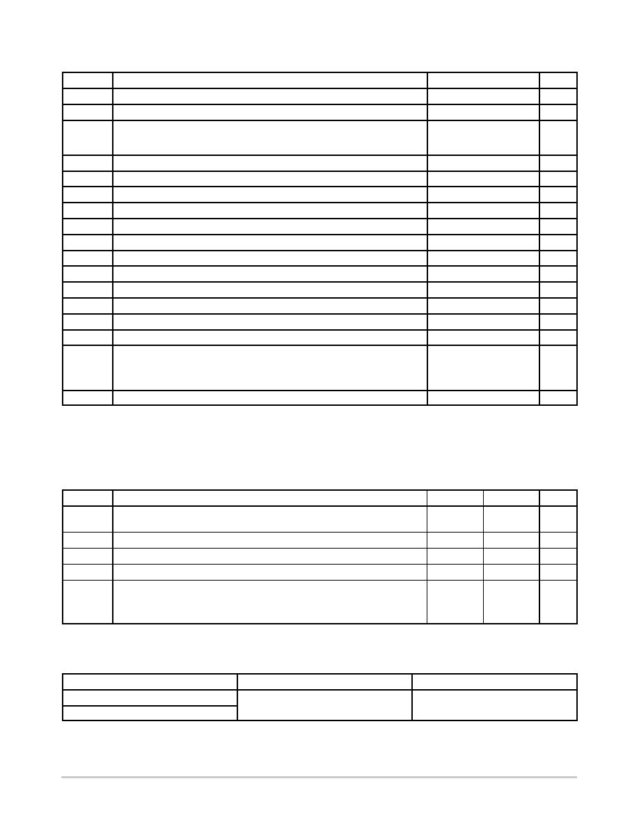
MAXIMUM RATINGS
Symbol
Parameter
Value
Units
VCC
DC Supply Voltage
0.5 to +7.0
V
VI
DC Input Voltage
0.5 to +7.0
V
VO
DC Output Voltage
Output in High Impedance State
Output in HIGH or LOW State
0.5 to +7.0
0.5 to VCC + 0.5
V
IIK
DC Input Diode Current, VI < GND
50
mA
IOK
DC Output Diode Current, VO < GND
50
mA
IO
DC Output Sink Current
±50
mA
ICC
DC Supply Current per Supply Pin
±100
mA
IGND
DC Ground Current per Ground Pin
±100
mA
TSTG
Storage Temperature Range
65 to +150
°C
TL
Lead Temperature, 1 mm from Case for 10 Seconds
260
°C
TJ
Junction Temperature under Bias
+150
°C
qJA
Thermal Resistance (Note 1)
250
°C/W
PD
Power Dissipation in Still Air at 85°C
250
mW
MSL
Moisture Sensitivity
Level 1
FR
Flammability Rating Oxygen Index: 28 to 34
UL 94 V0 @ 0.125 in
VESD
ESD Withstand Voltage
Human Body Model (Note 2)
Machine Model (Note 3)
Charged Device Model (Note 4)
> 2000
> 200
N/A
V
ILATCHUP
±100
mA
Stresses exceeding those listed in the Maximum Ratings table may damage the device. If any of these limits are exceeded, device functionality
should not be assumed, damage may occur and reliability may be affected.
1. Measured with minimum pad spacing on an FR4 board, using 10 mmby1 inch, 2ounce copper trace with no air flow.
2. Tested to EIA/JESD22A114A.
3. Tested to EIA/JESD22A115A.
4. Tested to JESD22C101A.
5. Tested to EIA/JESD78.
RECOMMENDED OPERATING CONDITIONS
Symbol
Parameter
Min
Max
Units
VCC
Supply Voltage
Operating
Data Retention Only
1.65
1.5
5.5
V
VI
Input Voltage (Note 6)
0
5.5
V
VO
Output Voltage (HIGH or LOW State)
0
5.5
V
TA
Operating FreeAir Temperature
55
+125
°C
Dt/DV
Input Transition Rise or Fall Rate
VCC = 2.5 V ±0.2 V
VCC = 3.0 V ±0.3 V
VCC = 5.0 V ±0.5 V
0
20
10
5
ns/V
Functional operation above the stresses listed in the Recommended Operating Ranges is not implied. Extended exposure to stresses beyond
the Recommended Operating Ranges limits may affect device reliability.
6. Unused inputs may not be left open. All inputs must be tied to a high or lowlogic input voltage level.
DEVICE ORDERING INFORMATION
Device Order Number
Package Type
Shipping
NL27WZ125USG
US8
(PbFree)
3000 / Tape & Reel
NLV27WZ125USG*
For information on tape and reel specifications, including part orientation and tape sizes, please refer to our Tape and Reel Packaging
Specifications Brochure, BRD8011/D.
*NLV Prefix for Automotive and Other Applications Requiring Unique Site and Control Change Requirements; AECQ100 Qualified and PPAP Capable.
相关PDF资料 |
PDF描述 |
|---|---|
| NL27WZ126US | IC BUFFER DL TRI-ST NON-INV US8 |
| NL27WZ16DTT1G | IC BUFFER DUAL NON-INVERT 6TSOP |
| NL27WZ17DFT2 | IC BUFF SCHM TRG DL N-INV SOT363 |
| NL37WZ07US | IC GATE INVERTER TRIPLE 1IN US8 |
| NL37WZ16US | IC BUFFER TRIPLE NON-INVERT US8 |
相关代理商/技术参数 |
参数描述 |
|---|---|
| NL27WZ125USG | 制造商:ON Semiconductor 功能描述:Buffer / Driver / Receiver Logic IC |
| NL27WZ126 | 制造商:ONSEMI 制造商全称:ON Semiconductor 功能描述:Dual Buffer with 3−State Outputs |
| NL27WZ126/D | 制造商:未知厂家 制造商全称:未知厂家 功能描述:Dual Buffer with 3-State Outputs |
| NL27WZ126_06 | 制造商:ONSEMI 制造商全称:ON Semiconductor 功能描述:Dual Buffer with 3−State Outputs |
| NL27WZ126_12 | 制造商:ONSEMI 制造商全称:ON Semiconductor 功能描述:Dual Buffer with 3-State Outputs |
发布紧急采购,3分钟左右您将得到回复。