- 您现在的位置:买卖IC网 > PDF目录189240 > NL74VCX16245DT (ON SEMICONDUCTOR) ALVC/VCX/A SERIES, DUAL 8-BIT TRANSCEIVER, TRUE OUTPUT, PDSO48 PDF资料下载
参数资料
| 型号: | NL74VCX16245DT |
| 厂商: | ON SEMICONDUCTOR |
| 元件分类: | 总线收发器 |
| 英文描述: | ALVC/VCX/A SERIES, DUAL 8-BIT TRANSCEIVER, TRUE OUTPUT, PDSO48 |
| 封装: | TSSOP-48 |
| 文件页数: | 7/12页 |
| 文件大小: | 267K |
| 代理商: | NL74VCX16245DT |
NL74VCX16245
http://onsemi.com
4
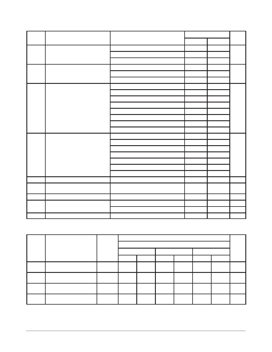
DC ELECTRICAL CHARACTERISTICS
TA = –40°C to +85°C
Symbol
Characteristic
Condition
Min
Max
Unit
VIH
HIGH Level Input Voltage (Note 2.)
1.65V
≤ VCC < 2.3V
0.65 x VCC
V
2.3V
≤ VCC ≤ 2.7V
1.6
2.7V < VCC ≤ 3.6V
2.0
VIL
LOW Level Input Voltage (Note 2.)
1.65V
≤ VCC < 2.3V
0.35 x VCC
V
2.3V
≤ VCC ≤ 2.7V
0.7
2.7V < VCC ≤ 3.6V
0.8
VOH
HIGH Level Output Voltage
1.65V
≤ VCC ≤ 3.6V; IOH = –100A
VCC – 0.2
V
VCC = 1.65V; IOH = –6mA
1.25
VCC = 2.3V; IOH = –6mA
2.0
VCC = 2.3V; IOH = –12mA
1.8
VCC = 2.3V; IOH = –18mA
1.7
VCC = 2.7V; IOH = –12mA
2.2
VCC = 3.0V; IOH = –18mA
2.4
VCC = 3.0V; IOH = –24mA
2.2
VOL
LOW Level Output Voltage
1.65V
≤ VCC ≤ 3.6V; IOL = 100A
0.2
V
VCC = 1.65V; IOL = 6mA
0.3
VCC = 2.3V; IOL = 12mA
0.4
VCC = 2.3V; IOL = 18mA
0.6
VCC = 2.7V; IOL = 12mA
0.4
VCC = 3.0V; IOL = 18mA
0.4
VCC = 3.0V; IOL = 24mA
0.55
II
Input Leakage Current
1.65V
≤ VCC ≤ 3.6V; 0V ≤ VI ≤ 3.6V
±5.0
A
IOZ
3–State Output Current
1.65V
≤ VCC ≤ 3.6V; 0V ≤ VO ≤ 3.6V;
VI = VIH or VIL
±10
A
IOFF
Power–Off Leakage Current
VCC = 0V; VI or VO = 3.6V
10
A
ICC
Quiescent Supply Current (Note 3.)
1.65V
≤ VCC ≤ 3.6V; VI = GND or VCC
20
A
1.65V
≤ VCC ≤ 3.6V; 3.6V ≤ VI, VO ≤ 3.6V
±20
A
ICC
Increase in ICC per Input
2.7V < VCC ≤ 3.6V; VIH = VCC – 0.6V
750
A
2. These values of VI are used to test DC electrical characteristics only.
3. Outputs disabled or 3–state only.
AC CHARACTERISTICS (Note 4.; tR = tF = 2.0ns; CL = 30pF; RL = 500)
Limits
TA = –40°C to +85°C
VCC = 3.0V to 3.6V
VCC = 2.3V to 2.7V
VCC = 1.65 to1.95V
Symbol
Parameter
Waveform
Min
Max
Min
Max
Min
Max
Unit
tPLH
tPHL
Propagation Delay
Input to Output
1
0.8
2.5
1.0
3.0
1.5
6.0
ns
tPZH
tPZL
Output Enable Time to
High and Low Level
2
0.8
3.8
1.0
4.9
1.5
9.3
ns
tPHZ
tPLZ
Output Disable Time From
High and Low Level
2
0.8
3.7
1.0
4.2
1.5
7.6
ns
tOSHL
tOSLH
Output–to–Output Skew
(Note 5.)
0.5
0.75
ns
4. For CL = 50pF, add approximately 300ps to the AC maximum specification.
5. Skew is defined as the absolute value of the difference between the actual propagation delay for any two separate outputs of the same device.
The specification applies to any outputs switching in the same direction, either HIGH–to–LOW (tOSHL) or LOW–to–HIGH (tOSLH);parameter
guaranteed by design.
相关PDF资料 |
PDF描述 |
|---|---|
| NLC565050T-6R8K-PF | 1 ELEMENT, 6.8 uH, GENERAL PURPOSE INDUCTOR, SMD |
| NLC565050T-561K-PF | 1 ELEMENT, 560 uH, GENERAL PURPOSE INDUCTOR, SMD |
| NLC565050T-4R7K-PF | 1 ELEMENT, 4.7 uH, GENERAL PURPOSE INDUCTOR, SMD |
| NLC565050T-471K-PF | 1 ELEMENT, 470 uH, GENERAL PURPOSE INDUCTOR, SMD |
| NLC565050T-390K-PF | 1 ELEMENT, 39 uH, GENERAL PURPOSE INDUCTOR, SMD |
相关代理商/技术参数 |
参数描述 |
|---|---|
| NL74VCX16245DTR2 | 制造商:未知厂家 制造商全称:未知厂家 功能描述:Dual 8-bit Bus Transceiver |
| NL74VCX16373DT | 制造商:未知厂家 制造商全称:未知厂家 功能描述:8-Bit D-Type Latch |
| NL74VCX16373DTR2 | 制造商:未知厂家 制造商全称:未知厂家 功能描述:8-Bit D-Type Latch |
| NL74VCX16374DT | 制造商:未知厂家 制造商全称:未知厂家 功能描述:16-Bit D-Type Flip-Flop |
| NL74VCX16374DTR2 | 制造商:未知厂家 制造商全称:未知厂家 功能描述:16-Bit D-Type Flip-Flop |
发布紧急采购,3分钟左右您将得到回复。