- 您现在的位置:买卖IC网 > PDF目录11441 > NLAST4599DTT1G (ON Semiconductor)IC SWITCH SPDT 6TSOP PDF资料下载
参数资料
| 型号: | NLAST4599DTT1G |
| 厂商: | ON Semiconductor |
| 文件页数: | 7/12页 |
| 文件大小: | 0K |
| 描述: | IC SWITCH SPDT 6TSOP |
| 标准包装: | 1 |
| 功能: | 开关 |
| 电路: | 1 x SPDT |
| 导通状态电阻: | 30 欧姆 |
| 电压电源: | 单电源 |
| 电压 - 电源,单路/双路(±): | 2 V ~ 5.5 V |
| 电流 - 电源: | 1µA |
| 工作温度: | -55°C ~ 125°C |
| 安装类型: | 表面贴装 |
| 封装/外壳: | SC-74,SOT-457 |
| 供应商设备封装: | 6-TSOP |
| 包装: | 标准包装 |
| 其它名称: | NLAST4599DTT1GOSDKR |
NLAST4599
http://onsemi.com
4
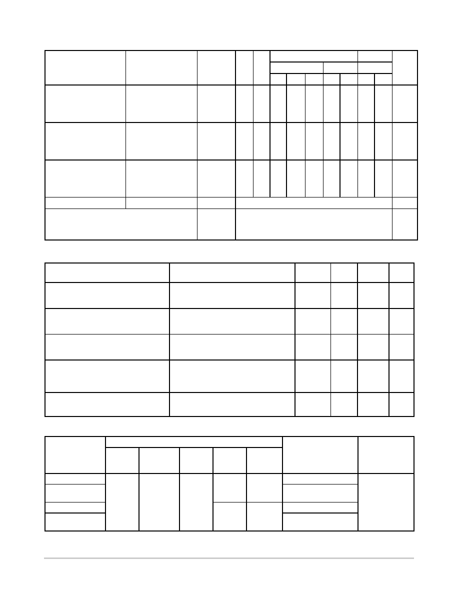
AC ELECTRICAL CHARACTERISTICS (Input tr = tf = 3.0 ns)
Parameter
Test Conditions
Symbol
Guaranteed Max Limit
Unit
VCC
VIS
55 to 25
_C
<85
_C
<125
_C
(V)
Min
Typ*
Max
Min
Max
Min
Max
TurnOn Time
RL = 300 W, CL = 35 pF
tON
2.5
3.0
4.5
5.5
2.0
3.0
5
2
23
16
11
9
28
21
16
14
5
2
30
25
20
5
2
30
25
20
ns
TurnOff Time
RL = 300 W, CL = 35 pF
tOFF
2.5
3.0
4.5
5.5
2.0
3.0
1
7
5
4
3
12
10
9
8
1
15
12
1
15
12
ns
Minimum BreakBefore
Make Time
RL = 300 W, CL = 35 pF
tBBM
2.5
3.0
4.5
5.5
2.0
3.0
1
12
11
6
5
1
ns
Typical @ 25, VCC = 5.0 V
Maximum Input Capacitance, Select Input
Analog I/O (switch off)
Common I/O (switch off)
Feedthrough (switch on)
CIN
CNO or CNC
CCOM
C(ON)
8
10
20
pF
*Typical Characteristics are at 25
_C.
ADDITIONAL APPLICATION CHARACTERISTICS (Voltages Referenced to GND Unless Noted)
Parameter
Condition
Symbol
VCC
V
Typical
25
°C
Unit
Maximum OnChannel 3dB Bandwidth or
Minimum Frequency Response
(Figure 10)
VIN = 0 dBm
VIN centered between VCC and GND
(Figure 7)
BW
3.0
4.5
5.5
170
200
MHz
Maximum Feedthrough On Loss
VIN = 0 dBm @ 100 kHz to 50 MHz
VIN centered between VCC and GND
(Figure 7)
VONL
3.0
4.5
5.5
2
dB
OffChannel Isolation
(Figure 10)
f = 100 kHz; VIS = 1 V RMS
VIN centered between VCC and GND
(Figure 7)
VISO
3.0
4.5
5.5
93
dB
Charge Injection Select Input to
Common I/O
(Figure 15)
VIN = VCC to GND, FIS = 20 kHz
tr = tf = 3 ns
RIS = 0 W, CL = 1000 pF
Q
3.0
5.5
1.5
3.0
pC
Total Harmonic Distortion
THD + Noise
(Figure 14)
FIS = 20 Hz to 100 kHz, RL = Rgen = 600 W,
CL = 50 pF
VIS = 5.0 VPP sine wave
THD
5.5
0.1
%
ORDERING INFORMATION
Device Nomenclature
Device
Circuit
Indicator
Technology
Device
Function
Package
Suffix
Tape &
Reel
Suffix
Package
Shipping
NLAST4599DFT2
NL
AS
4599
DF
T2
SC88/SC70/SOT363
3000/Tape & Reel
NLAST4599DFT2G
SC88/SC70/SOT363
(PbFree)
NLAST4599DTT1
DT
T1
TSOP6
NLAST4599DTT1G
TSOP6
(PbFree)
For information on tape and reel specifications, including part orientation and tape sizes, please refer to our Tape and Reel Packaging
Specifications Brochure, BRD8011/D.
相关PDF资料 |
PDF描述 |
|---|---|
| VE-JTL-IY-B1 | CONVERTER MOD DC/DC 28V 50W |
| DSPIC33EP64GP503T-I/TL | IC DSC 16BIT 64KB FLASH 36-VTLA |
| VE-J6F-IW-S | CONVERTER MOD DC/DC 72V 100W |
| VE-JVX-IY-B1 | CONVERTER MOD DC/DC 5.2V 50W |
| VE-J6D-IW-S | CONVERTER MOD DC/DC 85V 100W |
相关代理商/技术参数 |
参数描述 |
|---|---|
| NLAST4599DTT1G | 制造商:ON Semiconductor 功能描述:IC, ANALOG SWITCH, SINGLE, SPDT, TSOP-6 |
| NLAST4599DTT1G-CUT TAPE | 制造商:ON 功能描述:NLAST Series SPDT 5.5 V 85 Ohm Surface Mount Low Voltage Analog Switch - TSOP-6 |
| NLAST9431 | 制造商:ONSEMI 制造商全称:ON Semiconductor 功能描述:Low Voltage Single Supply Dual DPDT Analog Switch |
| NLAST9431MTR2G | 功能描述:模拟开关 IC ANA SWITCH RoHS:否 制造商:Texas Instruments 开关数量:2 开关配置:SPDT 开启电阻(最大值):0.1 Ohms 切换电压(最大): 开启时间(最大值): 关闭时间(最大值): 工作电源电压:2.7 V to 4.5 V 最大工作温度:+ 85 C 安装风格:SMD/SMT 封装 / 箱体:DSBGA-16 |
| NLASTV4599DFT2G | 制造商:ON Semiconductor 功能描述:SNGL SUPPLY DPDT SWITCH - Tape and Reel |
发布紧急采购,3分钟左右您将得到回复。