参数资料
| 型号: | NLSF302MNR2 |
| 厂商: | ON Semiconductor |
| 文件页数: | 2/4页 |
| 文件大小: | 0K |
| 描述: | IC GATE NOR QUAD CMOS 2INP 16QFN |
| 产品变化通告: | Product Discontinuation 31/Mar/2005 |
| 标准包装: | 3,000 |
| 逻辑类型: | 或非门 |
| 电路数: | 4 |
| 输入数: | 2 |
| 电源电压: | 2 V ~ 5.5 V |
| 电流 - 静态(最大值): | 2µA |
| 输出电流高,低: | 8mA,8mA |
| 逻辑电平 - 低: | 0.5V |
| 逻辑电平 - 高: | 1.5V |
| 额定电压和最大 CL 时的最大传播延迟: | 7.5ns @ 5V,50pF |
| 工作温度: | -40°C ~ 85°C |
| 安装类型: | 表面贴装 |
| 供应商设备封装: | 16-QFN(3x3) |
| 封装/外壳: | 16-VFQFN 裸露焊盘 |
| 包装: | 带卷 (TR) |
| 其它名称: | NLSF302MNR2OS |
NLSF302
http://onsemi.com
2
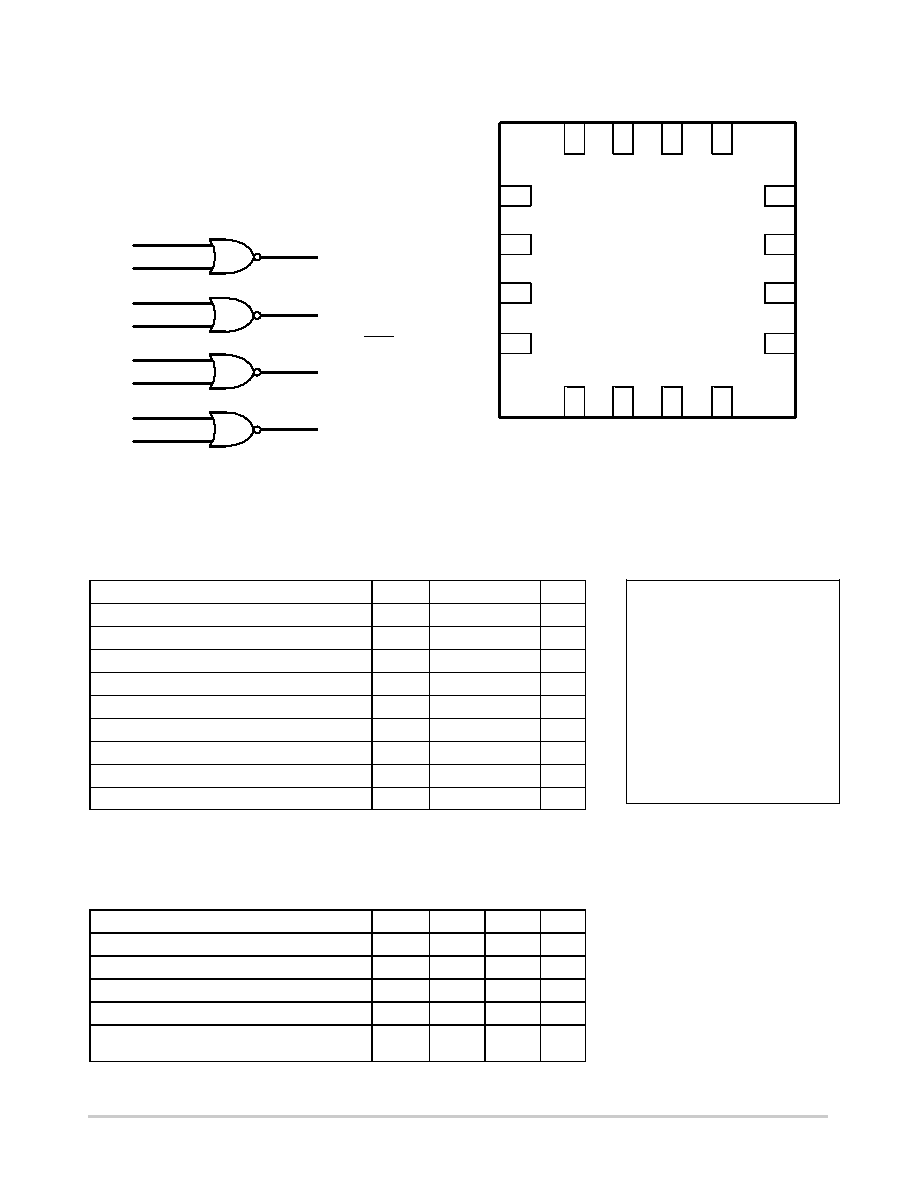
Figure 1. LOGIC DIAGRAM
1
5
Y1
16
A1
1
B1
Y4
Y = A + B
3
Y2
4
A2
5
B2
9
Y3
7
A3
8
B3
13
10
A4
12
B4
13
14
15
16
56
7
8
9
10
11
12
B3
B4
NC
A4
Y3
A3
GND
B2
Y4
V
CC
Y1
A1
B1
NC
Y2
A2
NLSF302
MN Package
(Top View)
1
2
3
4
Figure 2. PIN ASSIGNMENT (QFN16)
MAXIMUM RATINGS
Parameter
Symbol
Value
Unit
DC Supply Voltage
VCC
– 0.5 to + 7.0
V
DC Input Voltage
Vin
– 0.5 to + 7.0
V
DC Output Voltage
Vout
– 0.5 to VCC + 0.5
V
Input Diode Current
IIK
20
mA
Output Diode Current
IOK
± 20
mA
DC Output Current, per Pin
Iout
± 25
mA
DC Supply Current, VCC and GND Pins
ICC
± 50
mA
Power Dissipation in Still Air
PD
450
mW
Storage Temperature
Tstg
– 65 to + 150
°C
Stresses exceeding Maximum Ratings may damage the device. Maximum Ratings are stress
ratings only. Functional operation above the Recommended Operating Conditions is not implied.
Extended exposure to stresses above the Recommended Operating Conditions may affect
device reliability.
RECOMMENDED OPERATING CONDITIONS
Parameter
Symbol
Min
Max
Unit
DC Supply Voltage
VCC
2.0
5.5
V
DC Input Voltage
Vin
0
5.5
V
DC Output Voltage
Vout
0
VCC
V
Operating Temperature
TA
40
+85
°C
Input Rise and Fall Time
VCC = 3.3 V ± 0.3 V
VCC =5.0 V ± 0.5 V
tr, tf
0
100
20
ns/V
This device contains protection
circuitry to guard against damage
due to high static voltages or electric
fields. However, precautions must
be taken to avoid applications of any
voltage higher than maximum rated
voltages to this highimpedance cir-
cuit. For proper operation, Vin and
Vout should be constrained to the
range GND
v (Vin or Vout) v VCC.
Unused inputs must always be
tied to an appropriate logic voltage
level (e.g., either GND or VCC).
Unused outputs must be left open.
相关PDF资料 |
PDF描述 |
|---|---|
| NLSF308MNR2 | IC GATE AND QUAD CMOS 2INP 16QFN |
| NLU1G00BMX1TCG | IC GATE NAND SGL 2INPUT 6ULLGA |
| NLU1G04MUTCG | IC INVERTER SGL HS CMOS 6-UDFN |
| NLU1G08MUTCG | IC GATE AND SGL 2INP 6-UDFN |
| NLU1G14MUTCG | IC INVERTER SHCM TRIG SGL 6-UDFN |
相关代理商/技术参数 |
参数描述 |
|---|---|
| NLSF302MNR2G | 功能描述:逻辑门 LOG QUAD 2-INPUT NOR RoHS:否 制造商:Texas Instruments 产品:OR 逻辑系列:LVC 栅极数量:2 线路数量(输入/输出):2 / 1 高电平输出电流:- 16 mA 低电平输出电流:16 mA 传播延迟时间:3.8 ns 电源电压-最大:5.5 V 电源电压-最小:1.65 V 最大工作温度:+ 125 C 安装风格:SMD/SMT 封装 / 箱体:DCU-8 封装:Reel |
| NLSF308 | 制造商:ONSEMI 制造商全称:ON Semiconductor 功能描述:Quad 2−Input AND Gate |
| NLSF308/D | 制造商:未知厂家 制造商全称:未知厂家 功能描述:Quad 2-Input AND Gate |
| NLSF308_06 | 制造商:ONSEMI 制造商全称:ON Semiconductor 功能描述:Quad 2−Input AND Gate |
| NLSF308MNR2 | 功能描述:逻辑门 LOG QUAD 2 INPUT AND RoHS:否 制造商:Texas Instruments 产品:OR 逻辑系列:LVC 栅极数量:2 线路数量(输入/输出):2 / 1 高电平输出电流:- 16 mA 低电平输出电流:16 mA 传播延迟时间:3.8 ns 电源电压-最大:5.5 V 电源电压-最小:1.65 V 最大工作温度:+ 125 C 安装风格:SMD/SMT 封装 / 箱体:DCU-8 封装:Reel |
发布紧急采购,3分钟左右您将得到回复。