- 您现在的位置:买卖IC网 > Datasheet目录484 > NOIL2SC1300A-GDC (ON Semiconductor)IC IMAGE SENSOR LUPA1300 168PGA Datasheet资料下载
参数资料
| 型号: | NOIL2SC1300A-GDC |
| 厂商: | ON Semiconductor |
| 文件页数: | 17/45页 |
| 文件大小: | 0K |
| 描述: | IC IMAGE SENSOR LUPA1300 168PGA |
| 标准包装: | 18 |
| 系列: | * |
| 象素大小: | 14µm x 5.2µm |
| 有源象素阵列: | 1280H x 1024V |
| 每秒帧数: | 30 |
| 电源电压: | 2.5V, 3.3V |
| 类型: | CMOS 成像 |
| 封装/外壳: | * |
| 供应商设备封装: | * |
| 包装: | * |
第1页第2页第3页第4页第5页第6页第7页第8页第9页第10页第11页第12页第13页第14页第15页第16页当前第17页第18页第19页第20页第21页第22页第23页第24页第25页第26页第27页第28页第29页第30页第31页第32页第33页第34页第35页第36页第37页第38页第39页第40页第41页第42页第43页第44页第45页
�� �
�
�NOIL2SM1300A�
�Y2_start� (64� and� 65,� 10� bit).� These� registers� set� the� Y�
�start� address� for� window� 2� (if� enabled).�
�X2_start� (65,� 6bit).� This� register� sets� the� X� start� address�
�for� window� 2� (if� enabled).�
�Y2_end� (66� and� 67,� 10� bit).� These� registers� set� the� Y� end�
�address� for� window� 2� (if� enabled).�
�X2_kernels� (67,� 6� bit).� This� register� sets� the� number� of�
�kernels� or� X� width� to� be� read� out� for� window� 2� (if� enabled).�
�Y3_start� (68� and� 69,� 10� bit).� These� registers� set� the� Y�
�start� address� for� window� 3� (if� enabled).�
�X3_start� (69,� 6bit).� This� register� sets� the� X� start� address�
�for� window� 3� (if� enabled).�
�Y3_end� (70� and� 71,� 10� bit).� These� registers� set� the� Y� end�
�address� for� window� 3� (if� enabled).�
�X3_kernels� (71,� 6� bit).� This� register� sets� the� number� of�
�kernels� or� X� width� to� be� read� out� for� window� 3� (if� enabled).�
�Y4_start� (72� and� 73,� 10� bit).� These� registers� set� the� Y�
�start� address� for� window� 4� (if� enabled).�
�X4_start� (73,� 6bit).� This� register� sets� the� X� start� address�
�for� window� 4� (if� enabled).�
�Y4_end� (74� and� 75,� 10� bit).� These� registers� set� the� Y� end�
�address� for� window� 4� (if� enabled).�
�X4_kernels� (75,� 6� bit).� This� register� sets� the� number� of�
�kernels� or� X� width� to� be� read� out� for� window� 4� (if� enabled).�
�Res_length� (76� and� 77).� This� register� sets� the� length� of�
�the� internal� pixel� array� reset� (how� long� are� all� pixel� reset�
�simultaneously).� This� value� is� expressed� in� ’number� of�
�lines’� or� in� clock� cycles� (depends� on� seqmode3[6]).�
�Res_dsts_length.� This� register� sets� the� length� of� the�
�internal� dual� and� triple� slope� reset� pulses� when� enabled.� This�
�value� is� expressed� in� ’number� of� lines’� or� in� clock� cycles�
�(depends� on� seqmode3[6]).�
�Tint_timer� (79� and� 80).� This� register� sets� the� length� of�
�the� integration� time.� This� value� is� expressed� in� ’number� of�
�lines’� or� in� clock� cycles� (depends� on� seqmode3[6]).�
�Tint_ds_timer� (81� and� 82).� This� register� sets� the� length�
�of� the� dual� slope� integration� time.� This� value� is� expressed� in�
�’number� of� lines’� or� in� clock� cycles� (depends� on�
�seqmode3[6]).�
�Tint_ts_timer� (83� and� 84).� This� register� sets� the� length�
�of� the� triple� slope� integration� time.� This� value� is� expressed�
�in� ’number� of� lines’� or� in� clock� cycles� (depends� on�
�seqmode3[6]).�
�Serial� Peripheral� Interface� (SPI)�
�The� serial� 4-wire� interface� (or� SPI)� uses� a� serial� input� or�
�output� to� shift� the� data� in� or� out� the� register� buffer.� The� chip’s�
�configuration� registers� are� accessed� from� the� outside� world�
�through� the� SPI� protocol.� A� 4-wire� bus� runs� over� the� chip�
�and� connects� the� SPI� I/Os� with� the� internal� register� blocks.�
�To� upload� the� sensor,� follow� this� sequence:�
�Disable� Sequencer� ?� Upload� Sensor� for� new� setting� ?�
�Enable� Sequencer�
�When� sequencer� is� disabled,� the� training� pattern� appears�
�on� all� the� channels,� including� the� sync.� The� interface�
�consists� of:�
�?� cs_n:� chip� select,� when� LOW� the� chip� is� selected�
�?� clk:� the� spi� clock�
�?� in:� Master� out,� Slave� in,� the� serial� input� of� the� register�
�?� out:� Master� in,� Slave� out,� the� serial� output� of� the�
�register�
�SPI� Protocol�
�The� information� on� the� data� ‘in’� line� is:�
�?� A� command� bit� C,� indicating� a� write� (‘1’)� or� a� read�
�(‘0’)� access�
�?� 7-bit� address�
�?� 8-bit� data� word� (in� case� of� a� write� access)�
�The� data� ’out’� line� is� generally� in� High� Z� mode,� except�
�when� a� read� request� is� performed.�
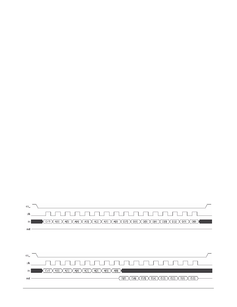
�Data� is� always� written� on� the� bus� on� the� falling� edge� of� the�
�clock,� and� sampled� on� the� rising� edge,� as� seen� in� Figure� 9� and�
�Figure� 10.� This� is� valid� for� both� the� ’in’� and� ’out’� bus.� The�
�system� clock� must� be� active� to� keep� the� SPI� uploads� stored�
�on� the� chip.� The� SPI� clock� speed� must� be� slower� by� a� factor�
�of� 30� when� compared� to� the� system� clock� (315� MHz� nominal�
�speed).�
�Figure� 9.� Write� Access� (C� =� ‘1’)�
�The� ‘out’� line� is� held� to� High� Z.� The� data� for� the� address�
�A� is� transferred� from� the� shift� register� to� the� active� register�
�register� block� with� address� A� can� write� its� data� on� the� ‘out’�
�bus.� The� data� on� ‘in’� is� ignored.�
�bank� (that� is,� sampled)� on� a� rising� edge� of� cs_n.� Only� the�
�Figure� 10.� Read� Access� (C� =� ‘0’)�
�http://onsemi.com�
�17�
�相关PDF资料 |
PDF描述 |
|---|---|
| NOIV1SE025KA-GDC | IC IMAGE SENSOR 25MP 355PGA |
| NP100P04PDG-E1-AY | MOSFET P-CH -40V MP-25ZP/TO-263 |
| NP100P04PLG-E1-AY | MOSFET P-CH -40V MP-25ZP/TO-263 |
| NP100P06PDG-E1-AY | MOSFET P-CH -60V MP-25ZP/TO-263 |
| NP100P06PLG-E1-AY | MOSFET P-CH -60V MP-25ZP/TO-263 |
相关代理商/技术参数 |
参数描述 |
|---|---|
| NOIL2SM1300A-GDC | 功能描述:IC IMAGE SENSOR LUPA1300 168PGA RoHS:是 类别:传感器,转换器 >> 图像,相机 系列:* 标准包装:480 系列:- 象素大小:6.7µm x 6.7µm 有源象素阵列:768H x 488V 每秒帧数:52 电源电压:3.3V 类型:CMOS 成像 封装/外壳:48-QFP 供应商设备封装:48-QFP 包装:托盘 请注意:* 配用:4H2105-ND - HEADBOARD FOR KAC-004014H2104-ND - KIT EVAL FOR KAC-00401 其它名称:4H20954H2095-NDKAC-00401-CBC-LB-A0 |
| NOIL2SM1300A-GWC | 功能描述:IC IMAGE SENSOR LUPA1300 168PGA RoHS:是 类别:传感器,转换器 >> 图像,相机 系列:* 标准包装:480 系列:- 象素大小:6.7µm x 6.7µm 有源象素阵列:768H x 488V 每秒帧数:52 电源电压:3.3V 类型:CMOS 成像 封装/外壳:48-QFP 供应商设备封装:48-QFP 包装:托盘 请注意:* 配用:4H2105-ND - HEADBOARD FOR KAC-004014H2104-ND - KIT EVAL FOR KAC-00401 其它名称:4H20954H2095-NDKAC-00401-CBC-LB-A0 |
| NOIS1SC1000A-HHC | 制造商:ON Semiconductor 功能描述:STAR1000 COLOR JLCC84 - Trays 制造商:ON Semiconductor 功能描述:IC IMAGE SENSOR STAR1000 84JLCC |
| NOIS1SM0250A-HHC | 制造商:ON Semiconductor 功能描述:STAR250 JLCC84 - Trays 制造商:ON Semiconductor 功能描述:IC IMAGE SENSOR STAR250 84JLCC |
| NOIS1SM0250A-WWC | 制造商:ON Semiconductor 功能描述:STAR250 WAFER SALES - Waffle Pack |
发布紧急采购,3分钟左右您将得到回复。