- 您现在的位置:买卖IC网 > PDF目录20508 > NSDEMN11XV6T1 (ON Semiconductor)DIODE SWITCH QUAD CC 80V SOT563 PDF资料下载
参数资料
| 型号: | NSDEMN11XV6T1 |
| 厂商: | ON Semiconductor |
| 文件页数: | 4/4页 |
| 文件大小: | 54K |
| 描述: | DIODE SWITCH QUAD CC 80V SOT563 |
| 产品变化通告: | Discontinuation 30/Jun/2006 |
| 标准包装: | 10 |
| 电压 - 在 If 时为正向 (Vf)(最大): | 1.2V @ 100mA |
| 电流 - 在 Vr 时反向漏电: | 100nA @ 70V |
| 电流 - 平均整流 (Io)(每个二极管): | 100mA(DC) |
| 电压 - (Vr)(最大): | 80V |
| 反向恢复时间(trr): | 4ns |
| 二极管类型: | 标准 |
| 速度: | 小信号 =< 200mA(Io),任意速度 |
| 二极管配置: | 2 对共阴极 |
| 安装类型: | 表面贴装 |
| 封装/外壳: | SOT-563,SOT-666 |
| 供应商设备封装: | SOT-563 |
| 包装: | 剪切带 (CT) |
| 工具箱: | SMSIGDIODEA-KIT-ND - KIT SMALL SIGNAL DIODE DESIGN |
| 其它名称: | NSDEMN11XV6T1OSCT |
NSDEMN11XV6T1, NSDEMN11XV6T5�
� http://onsemi.com�
� 4�
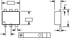
� PACKAGE DIMENSIONS�
� HE�
� DIM MIN NOM MAX�
� MILLIMETERS�
� A�
� 0.50 0.55 0.60�
� b�
� 0.17 0.22 0.27�
� C�
� D�
� 1.50 1.60 1.70�
� E�
� 1.10 1.20 1.30�
� e�
� 0.5 BSC�
� L�
� 0.10 0.20 0.30�
� 1.50 1.60 1.70�
� 0.020 0.021 0.023�
� 0.007 0.009 0.011�
� 0.059 0.062 0.066�
� 0.043 0.047 0.051�
� 0.02 BSC�
� 0.004 0.008 0.012�
� 0.059 0.062 0.066�
� MIN NOM MAX�
� INCHES�
� SOT?563, 6 LEAD�
� CASE 463A?01�
� ISSUE F�
� e�
� 0.08 (0.003)�
� M�
� X�
� Y�
� b�
� 6 5 PL�
� A�
� C�
� ?X?�
� ?Y?�
� NOTES:�
� 1. DIMENSIONING AND TOLERANCING PER ANSI�
� Y14.5M, 1982.�
� 2. CONTROLLING DIMENSION: MILLIMETERS�
� 3. MAXIMUM LEAD THICKNESS INCLUDES LEAD�
� FINISH THICKNESS. MINIMUM LEAD THICKNESS�
� IS THE MINIMUM THICKNESS OF BASE MATERIAL.�
� D�
� E�
� 12 3�
� 4�
� 5�
� L�
� 6�
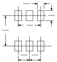
� 1.35�
� 0.0531�
� 0.5�
� 0.0197�
� 0.0197�
� SCALE 20:1�
� �
� mm�
� inches�
� 0.5�
� 1.0�
� 0.0394�
� 0.45�
� 0.0177�
� 0.3�
� 0.0118�
� *For additional information on our Pb?Free strategy and soldering�
� details, please download the ON Semiconductor Soldering and�
� Mounting Techniques Reference Manual, SOLDERRM/D.�
� SOLDERING FOOTPRINT*�
� HE�
� 0.08 0.12 0.18�
� 0.003 0.005 0.007�
� ON Semiconductor�
� and are registered trademarks of Semiconductor Components Industries, LLC (SCILLC). SCILLC reserves the right to mak�
� e changes without further notice�
� to any products herein. SCILLC makes no warranty, representation or guarantee regarding the suitability of its products for any particular purpose, nor does SCILLC assume any liability�
� arising out of the application or use of any product or circuit, and specifically disclaims any and all liability, including without limitation special, consequential or incidental damages.�
� “Typical” parameters which may be provided in SCILLC data sheets and/or specifications can and do vary in different applications and actual performance may vary over time. All�
� operating parameters, including “Typicals” must be validated for each customer application by customer’s technical experts. SCILLC does not convey any license under its patent rights�
� nor the rights of others. SCILLC products are not designed, intended, or authorized for use as components in systems intended for surgical implant into the body, or other applications�
� intended to support or sustain life, or for any other application in which the failure of the SCILLC product could create a situation where personal injury or death may occur. Should�
� Buyer purchase or use SCILLC products for any such unintended or unauthorized application, Buyer shall indemnify and hold SCILLC and its officers, employees, subsidiaries, affiliates,�
� and distributors harmless against all claims, costs, damages, and expenses, and reasonable attorney fees arising out of, directly or indirectly, any claim of personal injury or death�
� associated with such unintended or unauthorized use, even if such claim alleges that SCILLC was negligent regarding the design or manufacture of the part. SCILLC is an Equal�
� Opportunity/Affirmative Action Employer. This literature is subject to all applicable copyright laws and is not for resale in any manner.�
� PUBLICATION ORDERING INFORMATION�
� N. American Technical Support: 800?282?9855 Toll Free�
� USA/Canada�
� Europe, Middle East and Africa Technical Support:�
� Phone: 421 33 790 2910�
� Japan Customer Focus Center�
� Phone: 81?3?5773?3850�
� NSDEMN11XV6T1/D�
� LITERATURE FULFILLMENT:�
� Literature Distribution Center for ON Semiconductor�
� P.O. Box 5163, Denver, Colorado 80217 USA�
� Phone: 303?675?2175 or 800?344?3860 Toll Free USA/Canada�
� Fax: 303?675?2176 or 800?344?3867�
� Toll Free USA/Canada�
� Email: orderlit@onsemi.com�
� ON Semiconductor Website: www.onsemi.com�
� Order Literature: http://www.onsemi.com/orderlit�
� For additional information, please contact your local�
� Sales Representative�
�  �
�
� � �  �
�
� � �  �
�
� � �  �
�
� � �  �
�
� � �  �
�
� � �  �
�
� � 相关PDF资料 |
PDF描述 |
|---|---|
| VI-J33-CW-F1 | CONVERTER MOD DC/DC 24V 100W |
| EEM08DTMT | CONN EDGECARD 16POS R/A .156 SLD |
| FEP16GTA | DIODE FAST 400V 8A NEG TO220AB |
| AT24C11-10TI-2.7 | IC EEPROM 1KBIT 1MHZ 8TSSOP |
| R0.25D-153.3/HP-R | CONV DC/DC 0.25W 15V +/-3.3VOUT |
相关代理商/技术参数 |
参数描述 |
|---|---|
| NSDEMN11XV6T1G | 功能描述:二极管 - 通用,功率,开关 80V 100mA Quad Common Cathode RoHS:否 制造商:STMicroelectronics 产品:Switching Diodes 峰值反向电压:600 V 正向连续电流:200 A 最大浪涌电流:800 A 配置: 恢复时间:2000 ns 正向电压下降:1.25 V 最大反向漏泄电流:300 uA 最大功率耗散: 工作温度范围: 安装风格:SMD/SMT 封装 / 箱体:ISOTOP 封装:Tube |
| NSDEMN11XV6T5 | 功能描述:二极管 - 通用,功率,开关 80V 100mA Quad RoHS:否 制造商:STMicroelectronics 产品:Switching Diodes 峰值反向电压:600 V 正向连续电流:200 A 最大浪涌电流:800 A 配置: 恢复时间:2000 ns 正向电压下降:1.25 V 最大反向漏泄电流:300 uA 最大功率耗散: 工作温度范围: 安装风格:SMD/SMT 封装 / 箱体:ISOTOP 封装:Tube |
| NSDEMN11XV6T5G | 功能描述:二极管 - 通用,功率,开关 80V 100mA Quad Common Cathode RoHS:否 制造商:STMicroelectronics 产品:Switching Diodes 峰值反向电压:600 V 正向连续电流:200 A 最大浪涌电流:800 A 配置: 恢复时间:2000 ns 正向电压下降:1.25 V 最大反向漏泄电流:300 uA 最大功率耗散: 工作温度范围: 安装风格:SMD/SMT 封装 / 箱体:ISOTOP 封装:Tube |
| NSDEMP11XV6T1 | 功能描述:二极管 - 通用,功率,开关 80V 100mA Quad RoHS:否 制造商:STMicroelectronics 产品:Switching Diodes 峰值反向电压:600 V 正向连续电流:200 A 最大浪涌电流:800 A 配置: 恢复时间:2000 ns 正向电压下降:1.25 V 最大反向漏泄电流:300 uA 最大功率耗散: 工作温度范围: 安装风格:SMD/SMT 封装 / 箱体:ISOTOP 封装:Tube |
| NSDEMP11XV6T1/D | 制造商:未知厂家 制造商全称:未知厂家 功能描述:Common Anode Quad Array Switching Diode |
发布紧急采购,3分钟左右您将得到回复。