- 您现在的位置:买卖IC网 > PDF目录18868 > NTB35N15T4G (ON Semiconductor)MOSFET N-CH 150V 37A D2PAK PDF资料下载
参数资料
| 型号: | NTB35N15T4G |
| 厂商: | ON Semiconductor |
| 文件页数: | 1/8页 |
| 文件大小: | 0K |
| 描述: | MOSFET N-CH 150V 37A D2PAK |
| 标准包装: | 1 |
| FET 型: | MOSFET N 通道,金属氧化物 |
| FET 特点: | 标准 |
| 漏极至源极电压(Vdss): | 150V |
| 电流 - 连续漏极(Id) @ 25° C: | 37A |
| 开态Rds(最大)@ Id, Vgs @ 25° C: | 50 毫欧 @ 18.5A,10V |
| Id 时的 Vgs(th)(最大): | 4V @ 250µA |
| 闸电荷(Qg) @ Vgs: | 100nC @ 10V |
| 输入电容 (Ciss) @ Vds: | 3200pF @ 25V |
| 功率 - 最大: | 2W |
| 安装类型: | 表面贴装 |
| 封装/外壳: | TO-263-3,D²Pak(2 引线+接片),TO-263AB |
| 供应商设备封装: | D2PAK |
| 包装: | 剪切带 (CT) |
| 其它名称: | NTB35N15T4GOSCT |
��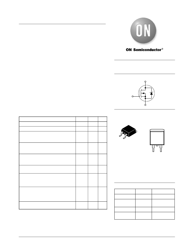 �
�
�NTB35N15�
�Power� MOSFET�
�37� Amps,� 150� Volts�
�N?Channel� Enhancement?Mode� D� 2� PAK�
�Features�
�?� Source?to?Drain� Diode� Recovery� Time� Comparable� to� a� Discrete�
�Fast� Recovery� Diode�
�?� Avalanche� Energy� Specified�
�?� I� DSS� and� R� DS(on)� Specified� at� Elevated� Temperature�
�?� Mounting� Information� Provided� for� the� D� 2� PAK� Package�
�?� Pb?Free� Packages� are� Available�
�Typical� Applications�
�http://onsemi.com�
�37� AMPERES,� 150� VOLTS�
�50� m� W� @� V� GS� =� 10� V�
�N?Channel�
�D�
�?� PWM� Motor� Controls�
�?� Power� Supplies�
�?� Converters�
�MAXIMUM� RATINGS� (T� J� =� 25� °� C� unless� otherwise� noted)�
�G�
�S�
�MARKING� DIAGRAM�
�&� PIN� ASSIGNMENT�
�Rating�
�Symbol�
�Value�
�Unit�
�Drain?to?Source� Voltage�
�V� DSS�
�150�
�Vdc�
�4�
�Drain?to?Source� Voltage� (R� GS� =� 1.0� M� W� )�
�V� DGR�
�150�
�Vdc�
�4�
�Drain�
�Gate?to?Source� Voltage�
�Vdc�
�?� Continuous�
�?� Non?Repetitive� (t� p� v� 10� ms)�
�V� GS�
�V� GSM�
�"� 20�
�"� 40�
�1�
�2�
�3�
�35N15G�
�AYWW�
�Drain� Current� ?� Continuous� @� T� A� =� 25� °� C�
�?� Continuous� @� T� A� =� 100� °� C�
�?� Pulsed� (Note� 2)�
�Total� Power� Dissipation� @� T� A� =� 25� °� C�
�Derate� above� 25� °� C�
�Total� Power� Dissipation� @� T� A� =� 25� °� C� (Note� 1)�
�I� D�
�I� D�
�I� DM�
�P� D�
�37�
�23�
�111�
�178�
�1.43�
�2.0�
�Adc�
�W�
�W/� °� C�
�W�
�D� 2� PAK�
�CASE� 418B�
�STYLE� 2�
�1�
�Gate�
�2�
�Drain�
�3�
�Source�
�Operating� and� Storage� Temperature� Range�
�Single� Pulse� Drain?to?Source� Avalanche�
�Energy� ?� Starting� T� J� =� 25� °� C�
�T� J� ,� T� stg�
�E� AS�
�?55� to�
�+150�
�700�
�°� C�
�mJ�
�35N15�
�A�
�Y�
�WW�
�G�
�=� Device� Code�
�=� Assembly� Location�
�=� Year�
�=� Work� Week�
�=� Pb?Free� Package�
�(V� DD� =� 100� Vdc,� V� GS� =� 10� Vdc,�
�I� L(pk)� =� 21.6� A,� L� =� 3.0� mH,� R� G� =� 25� W� )�
�ORDERING� INFORMATION�
�Thermal� Resistance�
�?� Junction?to?Case�
�?� Junction?to?Ambient�
�?� Junction?to?Ambient� (Note� 1)�
�Maximum� Lead� Temperature� for� Soldering�
�Purposes,� 1/8� in� from� case� for� 10� seconds�
�R� q� JC�
�R� q� JA�
�R� q� JA�
�T� L�
�0.7�
�62.5�
�50�
�260�
�°� C/W�
�°� C�
�Device�
�NTB35N15�
�NTB35N15G�
�Package�
�D� 2� PAK�
�D� 2� PAK�
�(Pb?Free)�
�Shipping� ?�
�50� Units/Rail�
�50� Units/Rail�
�Maximum� ratings� are� those� values� beyond� which� device� damage� can� occur.�
�Maximum� ratings� applied� to� the� device� are� individual� stress� limit� values� (not�
�NTB35N15T4�
�NTB35N15T4G�
�D� 2� PAK�
�D� 2� PAK�
�800� Tape� &� Reel�
�800� Tape� &� Reel�
�normal� operating� conditions)� and� are� not� valid� simultaneously.� If� these� limits� are�
�exceeded,� device� functional� operation� is� not� implied,� damage� may� occur� and�
�reliability� may� be� affected.�
�1.� When� surface� mounted� to� an� FR4� board� using� the� minimum� recommended�
�pad� size,� (Cu.� Area� 0.412� in� 2� ).�
�2.� Pulse� Test:� Pulse� Width� =� 10� m� s,� Duty� Cycle� =� 2%.�
�(Pb?Free)�
�?For� information� on� tape� and� reel� specifications,�
�including� part� orientation� and� tape� sizes,� please�
�refer� to� our� Tape� and� Reel� Packaging� Specification�
�Brochure,� BRD8011/D.�
�?� Semiconductor� Components� Industries,� LLC,� 2005�
�August,� 2005� ?� Rev.� 5�
�1�
�Publication� Order� Number:�
�NTB35N15/D�
�相关PDF资料 |
PDF描述 |
|---|---|
| ASDMB-11.0592MHZ-XY-T | OSC MEMS 11.0592 MHZ SMD |
| YGM1 C517 | THERM PTC MINI-BEAD 3MM 170C |
| YQD100N1000 | THERMISTOR PTC OCP 1000 OHM 25C |
| K50-HC0CSE25.0000MR | OSCILLATOR 25.00MHZ SMD |
| E33-50K | SWITCH ROLLER SPDT 10A QC TERM |
相关代理商/技术参数 |
参数描述 |
|---|---|
| NTB-3602 | 制造商:Quest Technology International Inc 功能描述: |
| NTB40603AS | 制造商:IKO NIPPON THOMPSON 功能描述:AXL NDL RLR 40MM |
| NTB4302 | 功能描述:MOSFET 30V 74A N-Channel RoHS:否 制造商:STMicroelectronics 晶体管极性:N-Channel 汲极/源极击穿电压:650 V 闸/源击穿电压:25 V 漏极连续电流:130 A 电阻汲极/源极 RDS(导通):0.014 Ohms 配置:Single 最大工作温度: 安装风格:Through Hole 封装 / 箱体:Max247 封装:Tube |
| NTB4302G | 功能描述:MOSFET 30V 74A N-Channel RoHS:否 制造商:STMicroelectronics 晶体管极性:N-Channel 汲极/源极击穿电压:650 V 闸/源击穿电压:25 V 漏极连续电流:130 A 电阻汲极/源极 RDS(导通):0.014 Ohms 配置:Single 最大工作温度: 安装风格:Through Hole 封装 / 箱体:Max247 封装:Tube |
| NTB4302T4 | 功能描述:MOSFET 30V 74A N-Channel RoHS:否 制造商:STMicroelectronics 晶体管极性:N-Channel 汲极/源极击穿电压:650 V 闸/源击穿电压:25 V 漏极连续电流:130 A 电阻汲极/源极 RDS(导通):0.014 Ohms 配置:Single 最大工作温度: 安装风格:Through Hole 封装 / 箱体:Max247 封装:Tube |
发布紧急采购,3分钟左右您将得到回复。