- 您现在的位置:买卖IC网 > PDF目录19184 > NTD18N06LT4G (ON Semiconductor)MOSFET N-CH 60V 18A DPAK PDF资料下载
参数资料
| 型号: | NTD18N06LT4G |
| 厂商: | ON Semiconductor |
| 文件页数: | 1/8页 |
| 文件大小: | 0K |
| 描述: | MOSFET N-CH 60V 18A DPAK |
| 标准包装: | 1 |
| FET 型: | MOSFET N 通道,金属氧化物 |
| FET 特点: | 逻辑电平门 |
| 漏极至源极电压(Vdss): | 60V |
| 电流 - 连续漏极(Id) @ 25° C: | 18A |
| 开态Rds(最大)@ Id, Vgs @ 25° C: | 65 毫欧 @ 9A,5V |
| Id 时的 Vgs(th)(最大): | 2V @ 250µA |
| 闸电荷(Qg) @ Vgs: | 22nC @ 5V |
| 输入电容 (Ciss) @ Vds: | 675pF @ 25V |
| 功率 - 最大: | 55W |
| 安装类型: | 表面贴装 |
| 封装/外壳: | TO-252-3,DPak(2 引线+接片),SC-63 |
| 供应商设备封装: | DPAK-3 |
| 包装: | 标准包装 |
| 其它名称: | NTD18N06LT4GOSDKR |
�� �
�
�NTD18N06L,� NTDV18N06L�
�Power� MOSFET�
�18� A,� 60� V,� Logic� Level� N� ?� Channel� DPAK�
�Designed� for� low� voltage,� high� speed� switching� applications� in�
�power� supplies,� converters� and� power� motor� controls� and� bridge�
�circuits.�
�http://onsemi.com�
�Features�
�?� AEC� Q101� Qualified� ?� NTDV18N06L�
�?� These� Devices� are� Pb� ?� Free� and� are� RoHS� Compliant�
�V� (BR)DSS�
�60� V�
�R� DS(on)� TYP�
�54� m� W@� 5.0� V�
�I� D� MAX�
�18� A�
�(Note� 1)�
�Typical� Applications�
�?�
�?�
�?�
�?�
�Power� Supplies�
�Converters�
�Power� Motor� Controls�
�Bridge� Circuits�
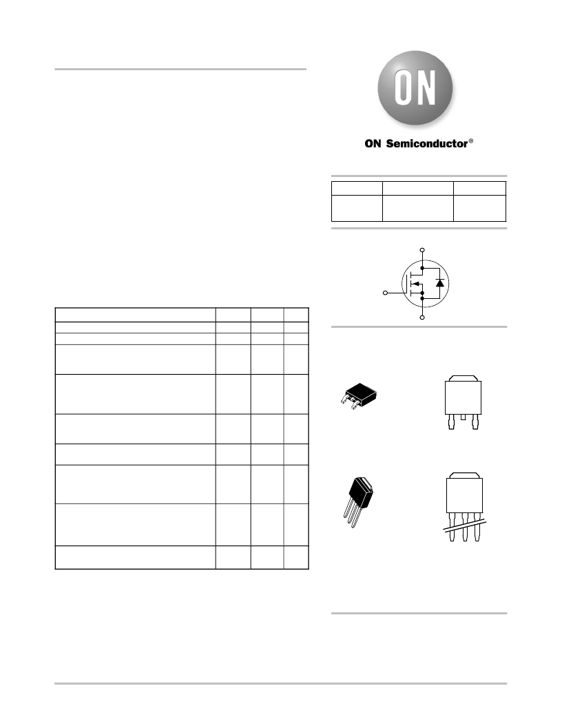
�N� ?� Channel�
�D�
�MAXIMUM� RATINGS� (T� J� =� 25� °� C� unless� otherwise� noted)�
�G�
�Rating�
�Drain� ?� to� ?� Source� Voltage�
�Drain� ?� to� ?� Gate� Voltage� (R� GS� =� 10� M� W� )�
�Gate� ?� to� ?� Source� Voltage�
�?� Continuous�
�?� Non� ?� repetitive� (t� p� v� 10� ms)�
�Symbol�
�V� DSS�
�V� DGR�
�V� GS�
�V� GS�
�Value�
�60�
�60�
�"� 15�
�"� 20�
�Unit�
�Vdc�
�Vdc�
�Vdc�
�S�
�MARKING�
�DIAGRAMS�
�4�
�Drain�
�1�
�3�
�Gate�
�Source�
�3�
�Drain� Current�
�?� Continuous� @� T� A� =� 25� °� C� I� D� 18� Adc�
�?� Continuous� @� T� A� =� 100� °� C� I� D� 10�
�?� Single� Pulse� (t� p� v� 10� m� s)� I� DM� 54� Apk�
�Total� Power� Dissipation� @� T� A� =� 25� °� C� P� D� 55� W�
�Derate� above� 25� °� C� 0.36� W/� °� C�
�Total� Power� Dissipation� @� T� A� =� 25� °� C� (Note� 2)� 2.1� W�
�Operating� and� Storage� Temperature� Range� T� J� ,� T� stg� ?� 55� to� °� C�
�+175�
�Single� Pulse� Drain� ?� to� ?� Source� Avalanche� E� AS� 72� mJ�
�Energy� ?� Starting� T� J� =� 25� °� C�
�(V� DD� =� 50� Vdc,� V� GS� =� 5.0� Vdc,�
�L� =� 1.0� mH,� I� L� (pk)� =� 12� A,� V� DS� =� 60� Vdc)�
�Thermal� Resistance� °� C/W�
�?� Junction� ?� to� ?� Case� R� q� JC� 2.73�
�?� Junction� ?� to� ?� Ambient� (Note� 1)� R� q� JA� 100�
�?� Junction� ?� to� ?� Ambient� (Note� 2)� R� q� JA� 71.4�
�Maximum� Lead� Temperature� for� Soldering� T� L� 260� °� C�
�Purposes,� 1/8� ″� from� case� for� 10� seconds�
�Stresses� exceeding� Maximum� Ratings� may� damage� the� device.� Maximum�
�Ratings� are� stress� ratings� only.� Functional� operation� above� the� Recommen-�
�ded� Operating� Conditions� is� not� implied.� Extended� exposure� to� stresses� above�
�the� Recommended� Operating� Conditions� may� affect� device� reliability.�
�1.� When� surface� mounted� to� an� FR� ?� 4� board� using� the� minimum� recommended�
�pad� size.�
�2.� When� surface� mounted� to� an� FR� ?� 4� board� using� the� 0.5� sq� in� drain� pad� size.�
�4�
�DPAK�
�CASE� 369C�
�1� 2� STYLE� 2�
�3�
�2�
�Drain�
�4�
�Drain�
�4�
�DPAK� ?� 3�
�CASE� 369D�
�STYLE� 2�
�1�
�2�
�1� 2� 3�
�Gate� Drain� Source�
�18N6L� =� Device� Code�
�Y� =� Year�
�WW� =� Work� Week�
�G� =� Pb� ?� Free� Device�
�ORDERING� INFORMATION�
�See� detailed� ordering� and� shipping� information� in� the� package�
�dimensions� section� on� page� 2� of� this� data� sheet.�
�?� Semiconductor� Components� Industries,� LLC,� 2011�
�August,� 2011� ?� Rev.� 6�
�1�
�Publication� Order� Number:�
�NTD18N06L/D�
�相关PDF资料 |
PDF描述 |
|---|---|
| 88970043 | CONTROL LOGIC 8I/O 120V DIN MNT |
| WC-GVH2630 | TOOL HAND CRIMP GVH 26-30AWG |
| ASVMPC-14.7456MHZ-LR-T | OSC 14.7456 MHZ CMOS MEMS SMD |
| SCA610-CC5H1A | ACCELEROMETER SNGL 3G DIL8 SMD |
| DP02T | PIANO STYLE DIP SWITCH |
相关代理商/技术参数 |
参数描述 |
|---|---|
| NTD18N06T4 | 功能描述:MOSFET 60V 18A N-Channel RoHS:否 制造商:STMicroelectronics 晶体管极性:N-Channel 汲极/源极击穿电压:650 V 闸/源击穿电压:25 V 漏极连续电流:130 A 电阻汲极/源极 RDS(导通):0.014 Ohms 配置:Single 最大工作温度: 安装风格:Through Hole 封装 / 箱体:Max247 封装:Tube |
| NTD18N06T4G | 功能描述:MOSFET 60V 18A N-Channel RoHS:否 制造商:STMicroelectronics 晶体管极性:N-Channel 汲极/源极击穿电压:650 V 闸/源击穿电压:25 V 漏极连续电流:130 A 电阻汲极/源极 RDS(导通):0.014 Ohms 配置:Single 最大工作温度: 安装风格:Through Hole 封装 / 箱体:Max247 封装:Tube |
| NTD20 | 制造商:EDI 制造商全称:Electronic devices inc. 功能描述:HIGH VOLTAGE-HIGH CURRENT SILICON RECTIFIERS |
| NTD20N03L27 | 功能描述:MOSFET 30V 20A N-Channel RoHS:否 制造商:STMicroelectronics 晶体管极性:N-Channel 汲极/源极击穿电压:650 V 闸/源击穿电压:25 V 漏极连续电流:130 A 电阻汲极/源极 RDS(导通):0.014 Ohms 配置:Single 最大工作温度: 安装风格:Through Hole 封装 / 箱体:Max247 封装:Tube |
| NTD20N03L27/D | 制造商:未知厂家 制造商全称:未知厂家 功能描述:Power MOSFET 20 Amps, 30 Volts |
发布紧急采购,3分钟左右您将得到回复。