- 您现在的位置:买卖IC网 > PDF目录18477 > NTD4863NAT4G (ON Semiconductor)MOSFET N-CH 25V 9.2A DPAK PDF资料下载
参数资料
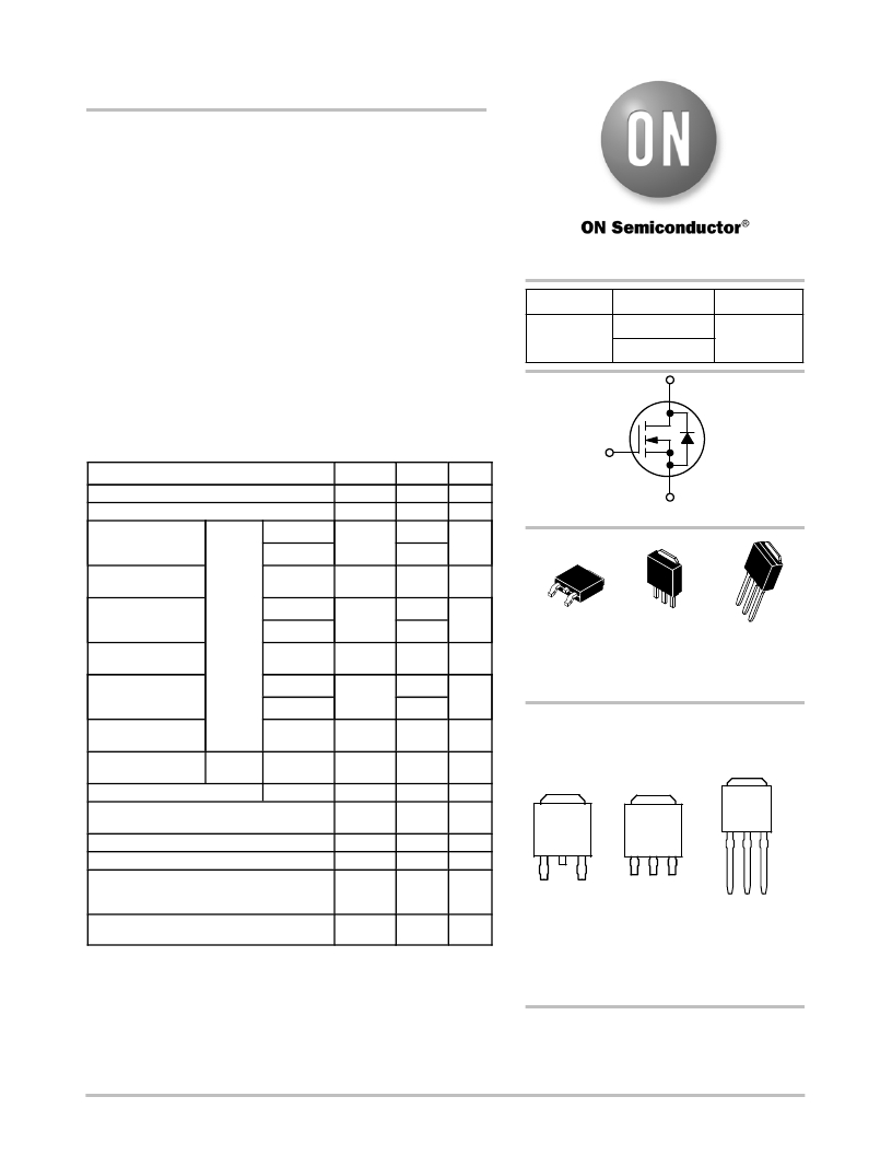
| 型号: | NTD4863NAT4G |
| 厂商: | ON Semiconductor |
| 文件页数: | 1/8页 |
| 文件大小: | 0K |
| 描述: | MOSFET N-CH 25V 9.2A DPAK |
| 标准包装: | 2,500 |
| FET 型: | MOSFET N 通道,金属氧化物 |
| FET 特点: | 逻辑电平门 |
| 漏极至源极电压(Vdss): | 25V |
| 电流 - 连续漏极(Id) @ 25° C: | 9.2A |
| 开态Rds(最大)@ Id, Vgs @ 25° C: | 9.3 毫欧 @ 30A,10V |
| Id 时的 Vgs(th)(最大): | 2.5V @ 250µA |
| 闸电荷(Qg) @ Vgs: | 13.5nC @ 4.5V |
| 输入电容 (Ciss) @ Vds: | 990pF @ 12V |
| 功率 - 最大: | 1.27W |
| 安装类型: | 表面贴装 |
| 封装/外壳: | TO-252-3,DPak(2 引线+接片),SC-63 |
| 供应商设备封装: | D-Pak |
| 包装: | 带卷 (TR) |
�� �
�
�NTD4863N�
�Power� MOSFET�
�25� V,� 49� A,� Single� N--Channel,� DPAK/IPAK�
�Features�
�?�
�Trench� Technology�
�?�
�?�
�Low� R� DS(on)� to� Minimize� Conduction� Losses�
�Low� Capacitance� to� Minimize� Driver� Losses�
�http://onsemi.com�
�?� Optimized� Gate� Charge� to� Minimize� Switching� Losses�
�?� These� are� Pb--Free� Devices�
�Applications�
�?� VCORE� Applications�
�?� DC--DC� Converters�
�V� (BR)DSS�
�25� V�
�R� DS(ON)� MAX�
�9.3� m� Ω� @� 10� V�
�14� m� Ω� @� 4.5� V�
�D�
�I� D� MAX�
�49� A�
�?� High� Side� Switching�
�MAXIMUM� RATINGS� (T� J� =� 25� °� C� unless� otherwise� stated)�
�G�
�Parameter�
�Symbol�
�Value�
�Unit�
�Drain--to--Source� Voltage�
�Gate--to--Source� Voltage�
�V� DSS�
�V� GS�
�25�
�±� 20�
�V�
�V�
�S�
�N--CHANNEL� MOSFET�
�2� 3�
�3�
�3�
�Continuous� Drain�
�Current� R� θ� JA�
�(Note� 1)�
�Power� Dissipation�
�R� θ� JA� (Note� 1)�
�Continuous� Drain�
�Current� R� θ� JA�
�(Note� 2)�
�Power� Dissipation�
�R� θ� JA� (Note� 2)�
�Continuous� Drain�
�Current� R� θ� JC�
�(Note� 1)�
�Power� Dissipation�
�R� θ� JC� (Note� 1)�
�Steady�
�State�
�T� A� =� 25� °� C�
�T� A� =� 85� °� C�
�T� A� =� 25� °� C�
�T� A� =� 25� °� C�
�T� A� =� 85� °� C�
�T� A� =� 25� °� C�
�T� C� =� 25� °� C�
�T� C� =� 85� °� C�
�T� C� =� 25� °� C�
�I� D�
�P� D�
�ID�
�P� D�
�I� D�
�P� D�
�11.3�
�8.8�
�1.95�
�9.2�
�7.1�
�1.27�
�49�
�38�
�36.6�
�A�
�W�
�A�
�W�
�A�
�W�
�1� 2� 1�
�4� 4�
�4�
�1�
�2�
�CASE� 369AA� CASE� 369AC� CASE� 369D�
�DPAK� 3� IPAK� IPAK�
�(Bent� Lead)� (Straight� Lead)� (Straight� Lead�
�STYLE� 2� DPAK)�
�MARKING� DIAGRAMS�
�&� PIN� ASSIGNMENTS�
�Pulsed� Drain� t� p� =10� m� s�
�Current�
�Current� Limited� by� Package�
�T� A� =� 25� °� C�
�T� A� =� 25� °� C�
�I� DM�
�I� DmaxPkg�
�98�
�35�
�A�
�A�
�4�
�Drain�
�4�
�Drain�
�4�
�Drain�
�Operating� Junction� and� Storage�
�Temperature�
�Source� Current� (Body� Diode)�
�Drain� to� Source� dV/dt�
�T� J� ,�
�T� STG�
�I� S�
�dV/dt�
�--55� to�
�+175�
�30.5�
�6�
�°� C�
�A�
�V/ns�
�1�
�2�
�3�
�Source� Gate� Drain� Source�
�1�
�2�
�3�
�Single� Pulse� Drain--to--Source� Avalanche� EAS� 60.5� mJ�
�Energy� (T� J� =� 25� °� C,� V� DD� =� 50� V,� V� GS� =� 10� V,�
�I� L� =� 11� A� pk� ,� L� =� 1.0� mH,� R� G� =� 25� Ω� )�
�Lead� Temperature� for� Soldering� Purposes� T� L� 260� °� C�
�(1/8”� from� case� for� 10� s)�
�Stresses� exceeding� Maximum� Ratings� may� damage� the� device.� Maximum�
�Ratings� are� stress� ratings� only.� Functional� operation� above� the� Recommended�
�Operating� Conditions� is� not� implied.� Extended� exposure� to� stresses� above� the�
�Recommended� Operating� Conditions� may� affect� device� reliability.�
�2�
�1� Drain� 3�
�Gate�
�Gate� Drain� Source�
�Y� =� Year�
�WW� =� Work� Week�
�4863N� =� Device� Code�
�G� =� Pb--Free� Package�
�ORDERING� INFORMATION�
�See� detailed� ordering� and� shipping� information� in� the� package�
�dimensions� section� on� page� 6� of� this� data� sheet.�
�?� Semiconductor� Components� Industries,� LLC,� 2010�
�June,� 2010� --� Rev.� 2�
�1�
�Publication� Order� Number:�
�NTD4863N/D�
�相关PDF资料 |
PDF描述 |
|---|---|
| ASG-D-X-B-125.000MHZ-T | OSC 125.00 MHZ 2.5V LVDS SMD |
| 3549S-1BD-103A | POT 10K OHM 7/8" RD WW |
| B82732F2601B001 | COIL CHOKE 68MH 600MA PIN |
| ASG-D-X-A-125.000MHZ-T | OSC 125.00 MHZ 3.3V LVDS SMD |
| AML22CBX3BB | SWITCH PUSHBUTTON SPDT 0.1A 125V |
相关代理商/技术参数 |
参数描述 |
|---|---|
| NTD4863NT4G | 功能描述:MOSFET NFET 25V 49A 0.0093R DPAK RoHS:否 制造商:STMicroelectronics 晶体管极性:N-Channel 汲极/源极击穿电压:650 V 闸/源击穿电压:25 V 漏极连续电流:130 A 电阻汲极/源极 RDS(导通):0.014 Ohms 配置:Single 最大工作温度: 安装风格:Through Hole 封装 / 箱体:Max247 封装:Tube |
| NTD4865N | 制造商:ONSEMI 制造商全称:ON Semiconductor 功能描述:Power MOSFET 25 V, 44 A, Single N-Channel, DPAK/IPAK |
| NTD4865N-1G | 功能描述:MOSFET PWR MSFT 25V 44A SINGLE N-CHNL RoHS:否 制造商:STMicroelectronics 晶体管极性:N-Channel 汲极/源极击穿电压:650 V 闸/源击穿电压:25 V 漏极连续电流:130 A 电阻汲极/源极 RDS(导通):0.014 Ohms 配置:Single 最大工作温度: 安装风格:Through Hole 封装 / 箱体:Max247 封装:Tube |
| NTD4865N-35G | 功能描述:MOSFET PWR MSFT 25V 44A SINGLE N-CHNL RoHS:否 制造商:STMicroelectronics 晶体管极性:N-Channel 汲极/源极击穿电压:650 V 闸/源击穿电压:25 V 漏极连续电流:130 A 电阻汲极/源极 RDS(导通):0.014 Ohms 配置:Single 最大工作温度: 安装风格:Through Hole 封装 / 箱体:Max247 封装:Tube |
| NTD4865NT4G | 功能描述:MOSFET PWR MSFT 25V 44A SINGLE N-CHNL RoHS:否 制造商:STMicroelectronics 晶体管极性:N-Channel 汲极/源极击穿电压:650 V 闸/源击穿电压:25 V 漏极连续电流:130 A 电阻汲极/源极 RDS(导通):0.014 Ohms 配置:Single 最大工作温度: 安装风格:Through Hole 封装 / 箱体:Max247 封装:Tube |
发布紧急采购,3分钟左右您将得到回复。