- 您现在的位置:买卖IC网 > PDF目录363711 > NTF5P03T3D (ON SEMICONDUCTOR) Power MOSFET PDF资料下载
参数资料
| 型号: | NTF5P03T3D |
| 厂商: | ON SEMICONDUCTOR |
| 英文描述: | Power MOSFET |
| 中文描述: | 功率MOSFET |
| 文件页数: | 6/8页 |
| 文件大小: | 69K |
| 代理商: | NTF5P03T3D |
NTF5P03T3
http://onsemi.com
6
TYPICAL ELECTRICAL CHARACTERISTICS
R
T
,
T
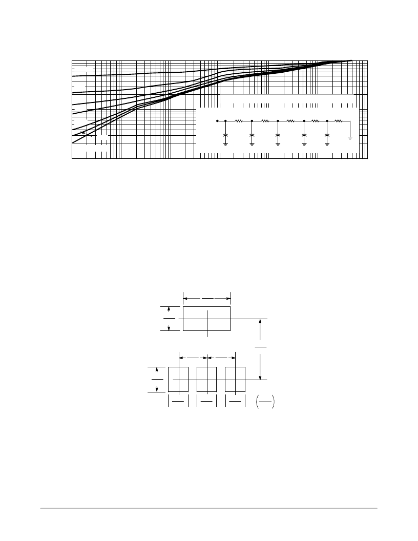
Figure 13. FET Thermal Response
t, TIME (s)
0.1
0.01
1.0E-03
D = 0.5
SINGLE PULSE
1.0E-02
1.0E-01
1.0E+00
1.0E+01
0.2
0.1
0.05
0.02
0.01
1.0E+02
1.0E+03
1
NORMALIZED TO R
JA
AT STEADY STATE (1
″
PAD)
CHIP
JUNCTION
0.0175
0.0154 F
0.0710
0.0854 F
0.2706
0.3074 F
0.5779
1.7891 F
0.7086
107.55 F
AMBIENT
INFORMATION FOR USING THE SOT–223 SURFACE MOUNT PACKAGE
MINIMUM RECOMMENDED FOOTPRINT FOR SURFACE MOUNTED APPLICATIONS
Surface mount board layout is a critical portion of the
total design. The footprint for the semiconductor packages
must be the correct size to insure proper solder connection
interface between the board and the package. With the
correct pad geometry, the packages will self align when
subjected to a solder reflow process.
0.079
2.0
0.15
3.8
0.248
6.3
0.079
2.0
0.059
1.5
0.059
1.5
0.059
1.5
0.091
2.3
0.091
2.3
mm
inches
相关PDF资料 |
PDF描述 |
|---|---|
| NTF6P02T3 | Power MOSFET -6.0 Amps, -20 Volts P–Channel SOT–223(-6.0A,-20V,P通道,SOT-23封装的功率MOSFET) |
| NTG103-39XX | High Accuracy NTC Thermistors |
| NTG104-36XX | High Accuracy NTC Thermistors |
| NTG104-41XX | High Accuracy NTC Thermistors |
| NTG403-35XX | High Accuracy NTC Thermistors |
相关代理商/技术参数 |
参数描述 |
|---|---|
| NTF5P03T3G | 功能描述:MOSFET 30V 5.2A P-Channel RoHS:否 制造商:STMicroelectronics 晶体管极性:N-Channel 汲极/源极击穿电压:650 V 闸/源击穿电压:25 V 漏极连续电流:130 A 电阻汲极/源极 RDS(导通):0.014 Ohms 配置:Single 最大工作温度: 安装风格:Through Hole 封装 / 箱体:Max247 封装:Tube |
| NTF5P03T3G | 制造商:ON Semiconductor 功能描述:TRANSISTOR |
| NTF6P02 | 制造商:ONSEMI 制造商全称:ON Semiconductor 功能描述:Power MOSFET -10 Amps, -20 Volts |
| NTF6P02T3 | 功能描述:MOSFET -20V -6A P-Channel RoHS:否 制造商:STMicroelectronics 晶体管极性:N-Channel 汲极/源极击穿电压:650 V 闸/源击穿电压:25 V 漏极连续电流:130 A 电阻汲极/源极 RDS(导通):0.014 Ohms 配置:Single 最大工作温度: 安装风格:Through Hole 封装 / 箱体:Max247 封装:Tube |
| NTF6P02T3/D | 制造商:未知厂家 制造商全称:未知厂家 功能描述:NTF6P02T3 |
发布紧急采购,3分钟左右您将得到回复。