- 您现在的位置:买卖IC网 > PDF目录18450 > NTLJD3182FZTAG (ON Semiconductor)MOSFET P-CH 20V 2.2A 6-WDFN PDF资料下载
参数资料
| 型号: | NTLJD3182FZTAG |
| 厂商: | ON Semiconductor |
| 文件页数: | 1/8页 |
| 文件大小: | 0K |
| 描述: | MOSFET P-CH 20V 2.2A 6-WDFN |
| 产品变化通告: | Product Obsolescence 21/Jan/2010 |
| 标准包装: | 3,000 |
| FET 型: | MOSFET P 通道,金属氧化物 |
| FET 特点: | 二极管(隔离式) |
| 漏极至源极电压(Vdss): | 20V |
| 电流 - 连续漏极(Id) @ 25° C: | 2.2A |
| 开态Rds(最大)@ Id, Vgs @ 25° C: | 100 毫欧 @ 2A,4.5V |
| Id 时的 Vgs(th)(最大): | 1V @ 250µA |
| 闸电荷(Qg) @ Vgs: | 7.8nC @ 4.5V |
| 输入电容 (Ciss) @ Vds: | 450pF @ 10V |
| 功率 - 最大: | 710mW |
| 安装类型: | 表面贴装 |
| 封装/外壳: | 6-WDFN 裸露焊盘 |
| 供应商设备封装: | 6-WDFN(2x2) |
| 包装: | 带卷 (TR) |
�� �
�
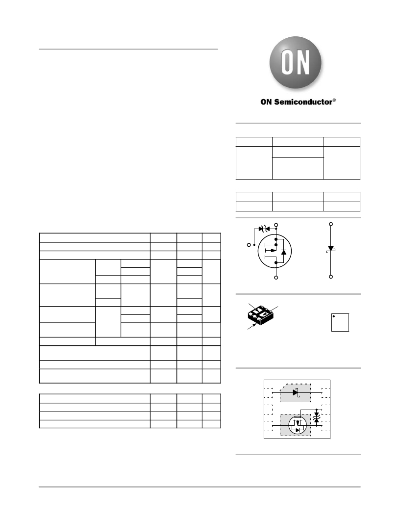
�NTLJD3182FZ�
�Power� MOSFET� and�
�Schottky� Diode�
�?� 20� V,� ?� 4.0� A,� m� Cool� t� Single� P� ?� Channel�
�&� Schottky� Barrier� Diode,� ESD�
�Features�
�?� WDFN� 2x2� mm� Package� with� Exposed� Drain� Pads� for� Excellent�
�Thermal� Conduction�
�?� Lowest� R� DS(on)� Solution� in� 2x2� mm� Package�
�?� Footprint� Same� as� SC� ?� 88� Package�
�?� Low� Profile� (<� 0.8� mm)� for� Easy� Fit� in� Thin� Environments�
�?� ESD� Protected�
�?� High� Current� Schottky� Diode:� 2� A� Current� Rating�
�?� This� is� a� Pb� ?� Free� Device�
�Applications�
�?� Optimized� for� Battery� and� Load� Management� Applications� in�
�Portable� Equipment�
�?� Li� ?� Ion� Battery� Charging� and� Protection� Circuits�
�?� DC� ?� DC� Buck� Circuit�
�MAXIMUM� RATINGS� (T� J� =� 25� °� C� unless� otherwise� noted)�
�V� (BR)DSS�
�?� 20� V�
�V� R� Max�
�20� V�
�http://onsemi.com�
�P� ?� CHANNEL� MOSFET�
�R� DS(on)� Max�
�100� m� W� @� ?� 4.5� V�
�144� m� W� @� ?� 2.5� V�
�200� m� W� @� ?� 1.8� V�
�SCHOTTKY� DIODE�
�V� F� Max�
�0.47� V�
�S� A�
�I� D� Max�
�?� 4.0� A�
�I� F� Max�
�2.0� A�
�Parameter�
�Symbol�
�Value�
�Unit�
�Drain� ?� to� ?� Source� Voltage�
�Gate� ?� to� ?� Source� Voltage�
�V� DSS�
�V� GS�
�?� 20�
�±� 8.0�
�V�
�V�
�G�
�Continuous� Drain�
�Current� (Note� 1)�
�Steady�
�State�
�t� ≤� 5s�
�T� A� =� 25� °� C�
�T� A� =� 85� °� C�
�T� A� =� 25� °� C�
�I� D�
�?� 3.2�
�?� 2.3�
�?� 4.0�
�A�
�D�
�K�
�MARKING�
�K�
�Power� Dissipation�
�(Note� 1)�
�Continuous� Drain�
�Current� (Note� 2)�
�Power� Dissipation�
�(Note� 2)�
�Steady�
�State�
�t� ≤� 5s�
�Steady�
�State�
�T� A� =� 25� °� C�
�T� A� =� 25� °� C�
�T� A� =� 85� °� C�
�T� A� =� 25� °� C�
�P� D�
�I� D�
�P� D�
�1.5�
�2.3�
�?� 2.2�
�?� 1.6�
�0.71�
�W�
�A�
�W�
�P� ?� CHANNEL� MOSFET� SCHOTTKY� DIODE�
�D�
�WDFN6� 1� 6�
�Pin� 1�
�DIAGRAM�
�CASE� 506AN� 2� JJM� G� 5�
�3� G� 4�
�Pulsed� Drain� Current� t� p� =� 10� m� s�
�Operating� Junction� and� Storage� Temperature�
�Source� Current� (Body� Diode)� (Note� 2)�
�Lead� Temperature� for� Soldering� Purposes�
�(1/8� ″� from� case� for� 10� s)�
�I� DM�
�T� J� ,� T� STG�
�I� S�
�T� L�
�?� 16�
�?� 55� to�
�150�
�?� 1.0�
�260�
�A�
�°� C�
�A�
�°� C�
�JJ� =� Specific� Device� Code�
�M� =� Date� Code�
�G� =� Pb� ?� Free� Package�
�(Note:� Microdot� may� be� in� either� location)�
�PIN� CONNECTIONS�
�SCHOTTKY MAXIMUM RATINGS� (T� J� = 2� 5� °� C� unless� otherwise� stated)�
�Parameter� Symbol� Value� Unit�
�A�
�1�
�K�
�6�
�K�
�Peak� Repetitive� Reverse� Voltage�
�DC� Blocking� Voltage�
�V� RRM�
�V� R�
�30�
�30�
�V�
�V�
�N/C�
�2�
�D�
�5�
�G�
�Average� Rectified� Forward� Current� I� F� 2.0� A�
�Stresses� exceeding� Maximum� Ratings� may� damage� the� device.� Maximum�
�Ratings� are� stress� ratings� only.� Functional� operation� above� the� Recommended�
�Operating� Conditions� is� not� implied.� Extended� exposure� to� stresses� above� the�
�Recommended� Operating� Conditions� may� affect� device� reliability.�
�D�
�3�
�(Top� View)�
�4�
�S�
�1.� Surface� Mounted� on� FR4� Board� using� 1� in� sq� pad� size� (Cu� area� =� 1.127� in� sq�
�[2� oz]� including� traces).�
�2.� Surface� Mounted� on� FR4� Board� using� the� minimum� recommended� pad� size,�
�(30� mm� 2� ,� 2� oz� Cu).�
�ORDERING� INFORMATION�
�See� detailed� ordering� and� shipping� information� in� the� package�
�dimensions� section� on� page� 3� of� this� data� sheet.�
�?� Semiconductor� Components� Industries,� LLC,� 2008�
�December,� 2008� ?� Rev.� 0�
�1�
�Publication� Order� Number:�
�NTLJD3180PZ/D�
�相关PDF资料 |
PDF描述 |
|---|---|
| ASG-P-X-A-1.500GHZ-T | OSC 1.500 GHZ 3.3V LVPECL SMD |
| PS1-200Q | SWITCH PUSHBUTTON DPDT 1A 125V |
| FDU6N50TU | MOSFET N-CH 500V 6A IPAK |
| PB-12331CG | SWITCH PUSHBUTTON SPDT 6A 125V |
| ASG-C-V-B-106.250MHZ | OSC 106.250 MHZ 2.5V LVCMOS SMD |
相关代理商/技术参数 |
参数描述 |
|---|---|
| NTLJD3182FZTBG | 功能描述:MOSFET 20V 4.1A UCOOL FETKY RoHS:否 制造商:STMicroelectronics 晶体管极性:N-Channel 汲极/源极击穿电压:650 V 闸/源击穿电压:25 V 漏极连续电流:130 A 电阻汲极/源极 RDS(导通):0.014 Ohms 配置:Single 最大工作温度: 安装风格:Through Hole 封装 / 箱体:Max247 封装:Tube |
| NTLJD3183CZ | 制造商:ONSEMI 制造商全称:ON Semiconductor 功能描述:Power MOSFET 20 V/−20 V, 4.7 A/−4.0 A, μCool? Complementary, 2x2 mm, WDFN Package |
| NTLJD3183CZTAG | 功能描述:MOSFET 20V 4.1A UCOOL CMPLM RoHS:否 制造商:STMicroelectronics 晶体管极性:N-Channel 汲极/源极击穿电压:650 V 闸/源击穿电压:25 V 漏极连续电流:130 A 电阻汲极/源极 RDS(导通):0.014 Ohms 配置:Single 最大工作温度: 安装风格:Through Hole 封装 / 箱体:Max247 封装:Tube |
| NTLJD3183CZTBG | 功能描述:MOSFET 20V 4.1A UCOOL CMPLM RoHS:否 制造商:STMicroelectronics 晶体管极性:N-Channel 汲极/源极击穿电压:650 V 闸/源击穿电压:25 V 漏极连续电流:130 A 电阻汲极/源极 RDS(导通):0.014 Ohms 配置:Single 最大工作温度: 安装风格:Through Hole 封装 / 箱体:Max247 封装:Tube |
| NTLJD4114N | 制造商:ONSEMI 制造商全称:ON Semiconductor 功能描述:High Efficiency DC-DC Converters |
发布紧急采购,3分钟左右您将得到回复。