- 您现在的位置:买卖IC网 > PDF目录18052 > NTMS7N03R2G (ON Semiconductor)MOSFET N-CH 30V 4.8A 8-SOIC PDF资料下载
参数资料
| 型号: | NTMS7N03R2G |
| 厂商: | ON Semiconductor |
| 文件页数: | 6/10页 |
| 文件大小: | 0K |
| 描述: | MOSFET N-CH 30V 4.8A 8-SOIC |
| 产品变化通告: | Wire Change 20/Aug/2008 |
| 标准包装: | 1 |
| FET 型: | MOSFET N 通道,金属氧化物 |
| FET 特点: | 逻辑电平门 |
| 漏极至源极电压(Vdss): | 30V |
| 电流 - 连续漏极(Id) @ 25° C: | 4.8A |
| 开态Rds(最大)@ Id, Vgs @ 25° C: | 23 毫欧 @ 7A,10V |
| Id 时的 Vgs(th)(最大): | 3V @ 250µA |
| 闸电荷(Qg) @ Vgs: | 43nC @ 10V |
| 输入电容 (Ciss) @ Vds: | 1190pF @ 25V |
| 功率 - 最大: | 800mW |
| 安装类型: | 表面贴装 |
| 封装/外壳: | 8-SOIC(0.154",3.90mm 宽) |
| 供应商设备封装: | 8-SOICN |
| 包装: | 标准包装 |
| 其它名称: | NTMS7N03R2GOSDKR |
�� �
�
�NTMS7N03R2�
�10�
�QT�
�1.2�
�1000�
�V� DD� =� 24� V�
�8�
�6�
�V� GS�
�1.0�
�0.8�
�100�
�I� D� =� 7� A�
�V� GS� =� 10� V�
�t� d(off)�
�t� f�
�t� r�
�4�
�Q1�
�Q2�
�I� D� =� 3.5� A�
�T� J� =� 25� °� C�
�0.6�
�10�
�t� d(on)�
�2�
�0.4�
�0�
�0�
�5�
�10�
�15�
�20�
�25�
�30�
�0�
�1�
�1�
�10�
�100�
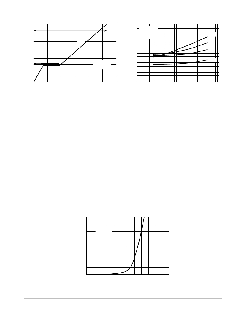
�Q� G� ,� TOTAL� GATE� CHARGE� (nC)�
�Figure� 8.� Gate?To?Source� and� Drain?To?Source�
�Voltage� versus� Total� Charge�
�R� G� ,� GATE� RESISTANCE� (OHMS)�
�Figure� 9.� Resistive� Switching� Time�
�Variation� versus� Gate� Resistance�
�DRAIN?TO?SOURCE� DIODE� CHARACTERISTICS�
�The� switching� characteristics� of� a� MOSFET� body� diode�
�are� very� important� in� systems� using� it� as� a� freewheeling� or�
�commutating� diode.� Of� particular� interest� are� the� reverse�
�recovery� characteristics� which� play� a� major� role� in�
�determining� switching� losses,� radiated� noise,� EMI� and� RFI.�
�System� switching� losses� are� largely� due� to� the� nature� of�
�the� body� diode� itself.� The� body� diode� is� a� minority� carrier�
�device,� therefore� it� has� a� finite� reverse� recovery� time,� t� rr� ,� due�
�to� the� storage� of� minority� carrier� charge,� Q� RR� ,� as� shown� in�
�the� typical� reverse� recovery� wave� form� of� Figure� 15.� It� is� this�
�stored� charge� that,� when� cleared� from� the� diode,� passes�
�through� a� potential� and� defines� an� energy� loss.� Obviously,�
�repeatedly� forcing� the� diode� through� reverse� recovery�
�further� increases� switching� losses.� Therefore,� one� would�
�like� a� diode� with� short� t� rr� and� low� Q� RR� specifications� to�
�minimize� these� losses.�
�The� abruptness� of� diode� reverse� recovery� effects� the�
�amount� of� radiated� noise,� voltage� spikes,� and� current�
�ringing.� The� mechanisms� at� work� are� finite� irremovable�
�circuit� parasitic� inductances� and� capacitances� acted� upon� by�
�8�
�7�
�high� di/dts.� The� diode’s� negative� di/dt� during� t� a� is� directly�
�controlled� by� the� device� clearing� the� stored� charge.�
�However,� the� positive� di/dt� during� t� b� is� an� uncontrollable�
�diode� characteristic� and� is� usually� the� culprit� that� induces�
�current� ringing.� Therefore,� when� comparing� diodes,� the�
�ratio� of� t� b� /t� a� serves� as� a� good� indicator� of� recovery�
�abruptness� and� thus� gives� a� comparative� estimate� of�
�probable� noise� generated.� A� ratio� of� 1� is� considered� ideal� and�
�values� less� than� 0.5� are� considered� snappy.�
�Compared� to� ON� Semiconductor� standard� cell� density�
�low� voltage� MOSFETs,� high� cell� density� MOSFET� diodes�
�are� faster� (shorter� t� rr� ),� have� less� stored� charge� and� a� softer�
�reverse� recovery� characteristic.� The� softness� advantage� of�
�the� high� cell� density� diode� means� they� can� be� forced� through�
�reverse� recovery� at� a� higher� di/dt� than� a� standard� cell�
�MOSFET� diode� without� increasing� the� current� ringing� or� the�
�noise� generated.� In� addition,� power� dissipation� incurred�
�from� switching� the� diode� will� be� less� due� to� the� shorter�
�recovery� time� and� lower� switching� losses.�
�6�
�5�
�4�
�3�
�2�
�1�
�0�
�V� GS� =� 0� V�
�T� J� =� 25� °� C�
�0.40�
�0.50�
�0.60�
�0.70�
�0.80�
�0.90�
�1.00�
�V� SD� ,� SOURCE?TO?DRAIN� VOLTAGE� (VOLTS)�
�Figure� 10.� Diode� Forward� Voltage� versus� Current�
�http://onsemi.com�
�6�
�相关PDF资料 |
PDF描述 |
|---|---|
| FCP0805H821J-J1 | CAP FILM 820PF 50VDC 0805 |
| PRQC8.00CR5010X000 | RESONATOR CER 8.00MHZ SMD |
| FCP0805H681J-J1 | CAP FILM 680PF 50VDC 0805 |
| FCP0805H561J-J1 | CAP FILM 560PF 50VDC 0805 |
| CSTCE12M0G55-R0 | CER RESONATOR 12.0MHZ SMD |
相关代理商/技术参数 |
参数描述 |
|---|---|
| NTMSD2P102LR2 | 功能描述:MOSFET 20V 3A P-Channel RoHS:否 制造商:STMicroelectronics 晶体管极性:N-Channel 汲极/源极击穿电压:650 V 闸/源击穿电压:25 V 漏极连续电流:130 A 电阻汲极/源极 RDS(导通):0.014 Ohms 配置:Single 最大工作温度: 安装风格:Through Hole 封装 / 箱体:Max247 封装:Tube |
| NTMSD2P102LR2/D | 制造商:未知厂家 制造商全称:未知厂家 功能描述:FETKY? |
| NTMSD2P102LR2_06 | 制造商:ONSEMI 制造商全称:ON Semiconductor 功能描述:NTMSD2P102LR2 |
| NTMSD2P102LR2G | 功能描述:MOSFET 20V 3A P-Channel RoHS:否 制造商:STMicroelectronics 晶体管极性:N-Channel 汲极/源极击穿电压:650 V 闸/源击穿电压:25 V 漏极连续电流:130 A 电阻汲极/源极 RDS(导通):0.014 Ohms 配置:Single 最大工作温度: 安装风格:Through Hole 封装 / 箱体:Max247 封装:Tube |
| NTMSD2P102R2 | 功能描述:MOSFET P-CH 20V 2.3A 8-SOIC RoHS:否 类别:分离式半导体产品 >> FET - 单 系列:- 标准包装:1,000 系列:MESH OVERLAY™ FET 型:MOSFET N 通道,金属氧化物 FET 特点:逻辑电平门 漏极至源极电压(Vdss):200V 电流 - 连续漏极(Id) @ 25° C:18A 开态Rds(最大)@ Id, Vgs @ 25° C:180 毫欧 @ 9A,10V Id 时的 Vgs(th)(最大):4V @ 250µA 闸电荷(Qg) @ Vgs:72nC @ 10V 输入电容 (Ciss) @ Vds:1560pF @ 25V 功率 - 最大:40W 安装类型:通孔 封装/外壳:TO-220-3 整包 供应商设备封装:TO-220FP 包装:管件 |
发布紧急采购,3分钟左右您将得到回复。