- 您现在的位置:买卖IC网 > Datasheet目录238 > NUP4114UCLW1T2G (ON Semiconductor)TVS ARRAY QUAD UNIDIR SC88 Datasheet资料下载
参数资料
| 型号: | NUP4114UCLW1T2G |
| 厂商: | ON Semiconductor |
| 文件页数: | 6/9页 |
| 文件大小: | 0K |
| 描述: | TVS ARRAY QUAD UNIDIR SC88 |
| 标准包装: | 3,000 |
| 电压 - 反向隔离(标准值): | 5.5V |
| 电压 - 击穿: | 6V |
| 电极标记: | 4 通道阵列 - 双向 |
| 安装类型: | 表面贴装 |
| 封装/外壳: | 6-TSSOP,SC-88,SOT-363 |
| 供应商设备封装: | SC-88 |
| 包装: | 带卷 (TR) |
�� �
�
�NUP4114� Series,� SZNUP4114HMR6T1G�
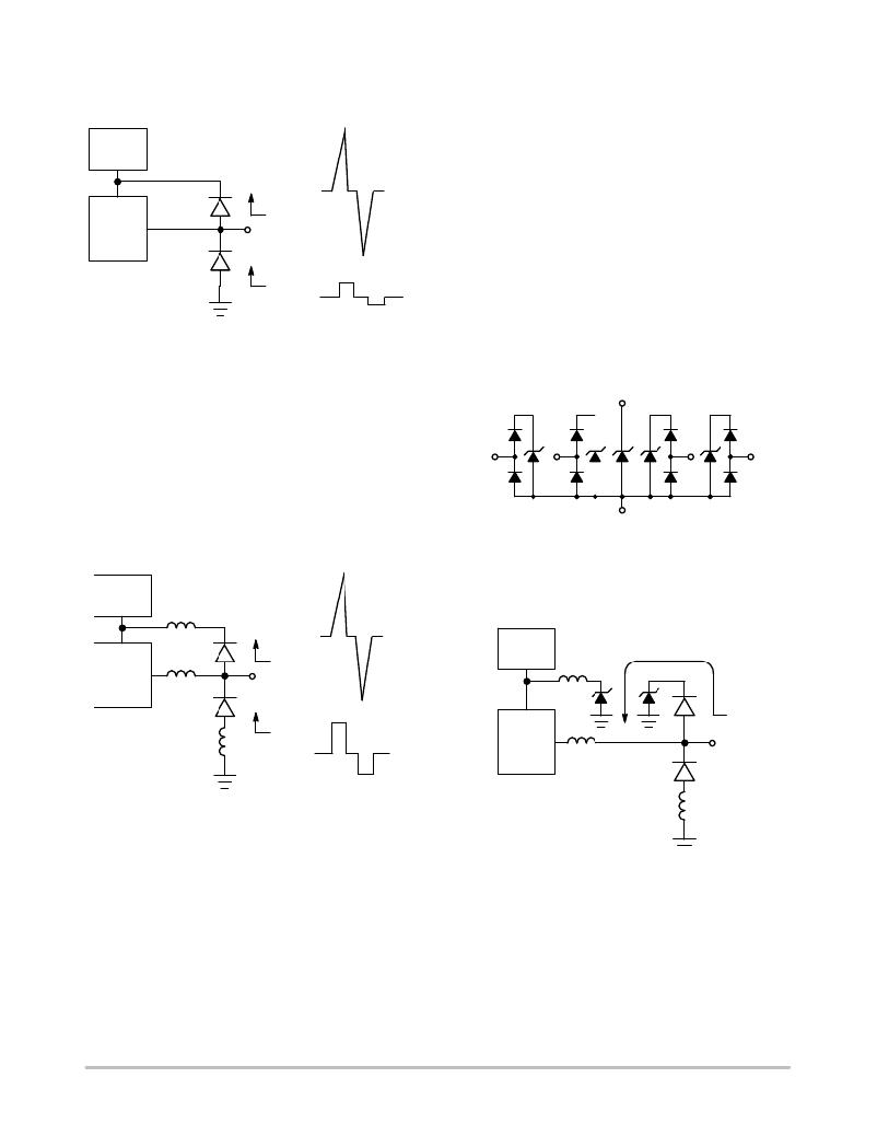
�Implementing� this� topology� with� discrete� devices� does� have�
�disadvantages.� This� configuration� is� shown� below:�
�layout.� Taking� care� to� minimize� the� effects� of� parasitic�
�inductance� will� provide� significant� benefits� in� transient�
�immunity.�
�Power�
�Supply�
�V� CC�
�I� ESDpos�
�Even� with� good� board� layout,� some� disadvantages� are� still�
�present� when� discrete� diodes� are� used� to� suppress� ESD�
�events� across� datalines� and� the� supply� rail.� Discrete� diodes�
�with� good� transient� power� capability� will� have� larger� die� and�
�Protected� Data� Line�
�Device�
�D1�
�D2�
�I� ESDpos�
�I� ESDneg�
�VF� +� V� CC�
�I� ESDneg�
�therefore� higher� capacitance.� This� capacitance� becomes�
�problematic� as� transmission� frequencies� increase.� Reducing�
�capacitance� generally� requires� reducing� die� size.� These�
�small� die� will� have� higher� forward� voltage� characteristics� at�
�typical� ESD� transient� current� levels.� This� voltage� combined�
�with� the� smaller� die� can� result� in� device� failure.�
�?� VF�
�Looking� at� the� figure� above,� it� can� be� seen� that� when� a�
�positive� ESD� condition� occurs,� diode� D1� will� be� forward�
�biased� while� diode� D2� will� be� forward� biased� when� a�
�negative� ESD� condition� occurs.� For� slower� transient�
�conditions,� this� system� may� be� approximated� as� follows:�
�For� positive� pulse� conditions:�
�The� ON� Semiconductor� NUP4114� was� developed� to�
�overcome� the� disadvantages� encountered� when� using�
�discrete� diodes� for� ESD� protection.� This� device� integrates� a�
�TVS� diode� within� a� network� of� steering� diodes.�
�5�
�V� c� =� V� CC� +� V� fD1�
�1�
�6�
�3�
�4�
�For� negative� pulse� conditions:�
�V� c� =� ?� V� fD2�
�ESD� events� can� have� rise� times� on� the� order� of� some�
�number� of� nanoseconds.� Under� these� conditions,� the� effect�
�of� parasitic� inductance� must� be� considered.� A� pictorial�
�representation� of� this� is� shown� below.�
�2�
�Figure� 7.� NUP4114� Equivalent� Circuit�
�Power�
�Supply�
�I� ESDpos�
�During� an� ESD� condition,� the� ESD� current� will� be� driven�
�to� ground� through� the� TVS� diode� as� shown� below.�
�V� CC�
�Protected�
�Device�
�Data� Line�
�D1�
�I� ESDpos�
�I� ESDneg�
�Power�
�Supply�
�V� CC�
�D2�
�V� C� =� V� CC� +� Vf� +� (L� diESD/dt)�
�I� ESDneg�
�Protected�
�D1�
�I� ESDpos�
�Device�
�Data� Line�
�D2�
�V� C� =� ?� Vf� ?� (L� diESD/dt)�
�An� approximation� of� the� clamping� voltage� for� these� fast�
�transients� would� be:�
�For� positive� pulse� conditions:�
�V� c� =� V� CC� +� Vf� +� (L� di� ESD� /dt)�
�For� negative� pulse� conditions:�
�V� c� =� ?� V� f� –� (L� di� ESD� /dt)�
�As� shown� in� the� formulas,� the� clamping� voltage� (V� c� )� not�
�only� depends� on� the� Vf� of� the� steering� diodes� but� also� on� the�
�L� di� ESD� /dt� factor.� A� relatively� small� trace� inductance� can�
�result� in� hundreds� of� volts� appearing� on� the� supply� rail.� This�
�endangers� both� the� power� supply� and� anything� attached� to�
�The� resulting� clamping� voltage� on� the� protected� IC� will�
�be:�
�V� c� =� V� F� +� V� TVS� .�
�The� clamping� voltage� of� the� TVS� diode� depends� on� the�
�magnitude� of� the� ESD� current.� The� steering� diodes� are� fast�
�switching� devices� with� unique� forward� voltage� and� low�
�capacitance� characteristics.�
�that� rail.� This� highlights� the� importance� of� good� board�
�http://onsemi.com�
�6�
�相关PDF资料 |
PDF描述 |
|---|---|
| NUP4201DR2G | IC TVS LO CAP HS DATA 500W 8SOIC |
| NUP4201MR6T1 | IC TVS DIODE ARRAY HS LINE 6TSOP |
| NUP4202W1T2G | IC TVS ARRAY HS DATALINE SOT-363 |
| NUP4212UPMUTAG | TVS QUAD ARRAY LOW CAP 6-UDFN |
| NUP4302MR6T1 | IC DIODE ARRAY SCHOTTKY TSOP6 |
相关代理商/技术参数 |
参数描述 |
|---|---|
| NUP4114UCW1 | 制造商:ONSEMI 制造商全称:ON Semiconductor 功能描述:Transient Voltage Suppressors |
| NUP4114UCW1_10 | 制造商:ONSEMI 制造商全称:ON Semiconductor 功能描述:Transient Voltage Suppressors |
| NUP4114UCW1T2G | 功能描述:TVS二极管阵列 TVS ARRAY RoHS:否 制造商:Littelfuse 极性: 通道:4 Channels 击穿电压: 钳位电压:11.5 V 工作电压:2.5 V 峰值浪涌电流:20 A 安装风格:SMD/SMT 端接类型:SMD/SMT 系列: 最小工作温度:- 40 C 最大工作温度:+ 85 C |
| NUP4114UPXV6 | 制造商:ONSEMI 制造商全称:ON Semiconductor 功能描述:Transient Voltage Suppressors |
| NUP4114UPXV6T1G | 功能描述:TVS二极管阵列 LOW CAP TVS ARRAY RoHS:否 制造商:Littelfuse 极性: 通道:4 Channels 击穿电压: 钳位电压:11.5 V 工作电压:2.5 V 峰值浪涌电流:20 A 安装风格:SMD/SMT 端接类型:SMD/SMT 系列: 最小工作温度:- 40 C 最大工作温度:+ 85 C |
发布紧急采购,3分钟左右您将得到回复。