参数资料
| 型号: | NUS6189MNTWG |
| 厂商: | ON Semiconductor |
| 文件页数: | 3/14页 |
| 文件大小: | 0K |
| 描述: | IC OVP LOW PRO W/MOSFET 22-QFN |
| 产品变化通告: | Product Obsolescence 21/Jan/2010 |
| 标准包装: | 3,000 |
| 技术: | 混合技术 |
| 电路数: | 1 |
| 应用: | 通用 |
| 封装/外壳: | 22-VFQFN 裸露焊盘 |
| 供应商设备封装: | 22-QFN(3x4) |
| 包装: | 带卷 (TR) |
�� �
�
�NUS6189MN�
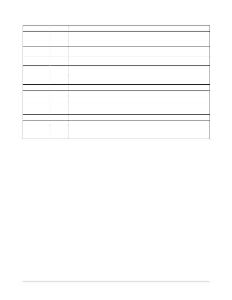
�FUNCTIONAL� PIN� DESCRIPTIONS�
�Pin�
�1�
�2,� 16,� 17,� 21,� 22�
�3�
�4,� 5,� 6,� 7�
�8�
�9,� 11,� 13�
�10�
�12�
�14�
�15�
�18�
�19�
�20�
�Function�
�Source� 1�
�Batt�
�Base�
�Collector�
�Emitter�
�OVP� OUT�
�Gate2�
�Source� 2�
�V� CC�
�V� IN�
�Gate1�
�Gnd�
�Control�
�Description�
�This� pin� is� the� source� of� MOSFET1� and� connects� to� the� more� negative� Vsense� pin� of� the� PMIC� and�
�to� the� more� negative� side� of� the� current� sense� resistor.�
�These� pins� are� the� drain� of� MOSFET2� and� connect� to� the� battery� and� the� Vbat� pin� of� the� PMIC.�
�The� base� of� the� internal� bipolar� transistor� is� connected� to� this� pin.� It� connects� to� the� Charge� Control�
�pin� of� the� PMIC.�
�The� collector� of� the� internal� bipolar� transistor� connects� to� these� pins� and� should� be� connected� to� the�
�more� positive� side� of� the� current� sense� resistor� as� well� as� the� more� positive� Vsense� pin� of� the� PMIC.�
�This� pin� is� connected� to� the� emitter� of� the� bipolar� transistor.� It� should� be� connected� externally� to� the�
�OVP� OUT� pins.�
�These� pins� are� the� output� of� the� OVP� circuit.� Internally� they� connect� to� the� drain� of� MOSFET2.� These�
�pins� connect� externally� to� the� Vcharge� pin� of� the� PMIC.�
�This� pin� is� the� gate� of� MOSFET2.� It� is� not� normally� connected� to� external� circuitry.�
�The� source� of� the� OVP� FET� is� connected� to� this� pin.� This� pin� needs� to� be� connected� to� pins� 14� &� 15.�
�This� pin� is� the� V� CC� pin� of� the� OVP� chip.� It� needs� to� be� connected� to� pins� 12� and� 15.�
�This� pin� senses� the� output� voltage� of� the� charger.� If� the� voltage� on� this� input� rises� above� the� over-�
�voltage� threshold� (V� TH� ),� the� OVP� OUT� pin� will� be� driven� to� within� 1.0� V� of� V� IN� ,� thus� disconnecting� the�
�FET.� The� nominal� threshold� level� is� 6.85� V.� This� pin� needs� to� be� connected� to� pins� 12� and� 14.�
�This� pin� is� the� gate� of� MOSFET1.� It� connects� to� the� Bat� FET� pin� of� the� PMIC.�
�This� is� the� ground� reference� pin� for� the� OVP� chip.�
�This� logic� signal� is� used� to� control� the� state� of� OVP� OUT� and� turn� ?� on/off� the� P� ?� channel� MOSFET.� A�
�logic� level� high� results� in� the� OVP� OUT� signal� being� driven� to� within� 1.0� V� of� VCC� which� turns� off�
�MOSFET2.� If� this� pin� is� not� used,� it� should� be� connected� to� ground.�
�http://onsemi.com�
�3�
�相关PDF资料 |
PDF描述 |
|---|---|
| OCB100CZ | BOARD CALIBR WIRED OPTO ASSY |
| OM10049 | EMULATOR PROGRAMMER LPC9X MCU |
| OPAMPEVM-PDIP | UNIV EVAL MOD FOR DIP PKG |
| OPB780KIT | KIT COLOR SENSOR OPB780Z |
| OPENLPPOL-EVB | BOARD EVAL OPEN-LOOP POL |
相关代理商/技术参数 |
参数描述 |
|---|---|
| NUSC2WC-WH | 制造商:Cooper Bussmann 功能描述:NUSC2 WHITE W/COVER - Bulk 制造商:COOPER INDUSTRIES 功能描述:NUSC2 WHITE W/COVER 制造商:COOPER BUSSMANN 功能描述:NUSC2 WHITE W/COVER |
| NUSC2-WH | 功能描述:接线端子 - 未指定 TERM BLOCK WHITE RoHS:否 制造商:Phoenix Contact 类型:Component Plug 位置/触点数量:2 电压额定值:24 V |
| NUSC4WC-WH | 制造商:Cooper Bussmann 功能描述:NUSC SERIES TERMINAL BLOCKS W/COVER - Bulk 制造商:COOPER BUSSMANN 功能描述:NUSC SERIES TERMINAL BLOCKS W/COVER |
| NUSC4-WH | 功能描述:接线端子 - 未指定 TERM BLOCK WHITE RoHS:否 制造商:Phoenix Contact 类型:Component Plug 位置/触点数量:2 电压额定值:24 V |
| NUSC6WC-WH | 功能描述:接线端子 - 未指定 TERM BLK BLACK NOREL RoHS:否 制造商:Phoenix Contact 类型:Component Plug 位置/触点数量:2 电压额定值:24 V |
发布紧急采购,3分钟左右您将得到回复。