参数资料
| 型号: | OP184ESZ |
| 厂商: | Analog Devices Inc |
| 文件页数: | 10/24页 |
| 文件大小: | 0K |
| 描述: | IC OPAMP GP R-R 4.25MHZ LN 8SOIC |
| 产品培训模块: | Top Five Problems in Photodiode Opamp Circuits |
| 设计资源: | Variable Gain Noninverting Amplifier Using AD5292 and OP184 (CN0112) Variable Gain Inverting Amplifier Using AD5292 and OP184 (CN0113) Programmable High Voltage Source with Boosted Output Current Using AD5292, OP184, and MOSFETs (CN0115) Low-Noise Microwave fractional-N PLL using active loop filter and RF prescaler (CN0174) |
| 标准包装: | 98 |
| 放大器类型: | 通用 |
| 电路数: | 1 |
| 输出类型: | 满摆幅 |
| 转换速率: | 4 V/µs |
| 增益带宽积: | 4.25MHz |
| 电流 - 输入偏压: | 80nA |
| 电压 - 输入偏移: | 100µV |
| 电流 - 电源: | 2.25mA |
| 电流 - 输出 / 通道: | 10mA |
| 电压 - 电源,单路/双路(±): | 3 V ~ 36 V,±1.5 V ~ 18 V |
| 工作温度: | -40°C ~ 125°C |
| 安装类型: | 表面贴装 |
| 封装/外壳: | 8-SOIC(0.154",3.90mm 宽) |
| 供应商设备封装: | 8-SO |
| 包装: | 管件 |
| 产品目录页面: | 774 (CN2011-ZH PDF) |
OP184/OP284/OP484
Rev. J | Page 18 of 24
HIGH-SIDE CURRENT MONITOR
In the design of power supply control circuits, a great deal of design
effort is focused on ensuring the long-term reliability of a pass
transistor over a wide range of load current conditions. As a result,
monitoring and limiting device power dissipation is of prime
importance in these designs. The circuit shown in Figure 55 is
an example of a 3 V, single-supply, high-side current monitor that
can be incorporated into the design of a voltage regulator with
fold-back current limiting or a high current power supply with
crowbar protection. This design uses an OP284 rail-to-rail input
voltage range to sense the voltage drop across a 0.1 Ω current shunt.
A P-channel MOSFET, used as the feedback element in the circuit,
converts the differential input voltage of the op amp into a current.
This current is applied to R2 to generate a voltage that is a linear
representation of the load current. The transfer equation for the
current monitor is given by
Monitor Output =
L
SENSE
I
R1
R
R2
×
×
For the element values shown, the transfer characteristic of the
monitor output is 2.5 V/A.
00293-
055
RSENSE
0.1
IL
8
1
4
3
3V
G
S
D
2
M1
SI9433
MONITOR
OUTPUT
3V
1/2
OP284
R1
100
R2
2.49k
0.1F
Figure 55. High-Side Load Current Monitor
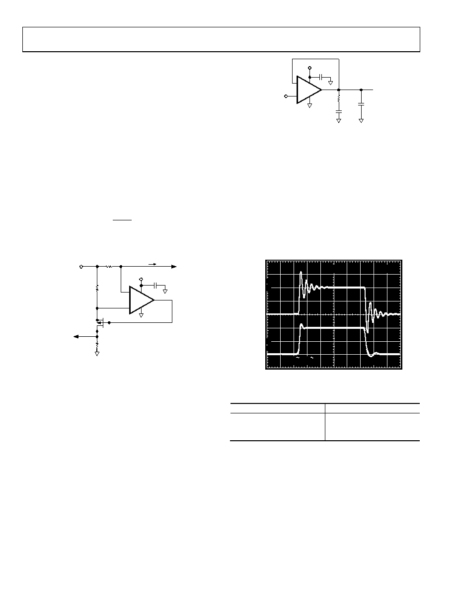
CAPACITIVE LOAD DRIVE CAPABILITY
The OP284 exhibits excellent capacitive load driving capabilities.
It can drive up to 1 nF, as shown in Figure 30. Even though the
device is stable, a capacitive load does not come without penalty in
bandwidth. The bandwidth is reduced to less than 1 MHz for loads
greater than 2 nF. A snubber network on the output does not
increase the bandwidth, but it does significantly reduce the amount
of overshoot for a given capacitive load.
A snubber consists of a series R-C network (RS, CS), as shown in
Figure 56, connected from the output of the device to ground.
This network operates in parallel with the load capacitor, CL, to
provide the necessary phase lag compensation. The value of the
resistor and capacitor is best determined empirically.
00293-
056
RS
50
0.1F
CL
1nF
CS
100nF
5V
VIN
100mV p-p
VOUT
1/2
OP284
Figure 56. Snubber Network Compensates for Capacitive Load
The first step is to determine the value of Resistor RS. A good
starting value is 100 Ω (typically, the optimum value is less than
100 Ω). This value is reduced until the small-signal transient
response is optimized. Next, CS is determined; 10 μF is a good
starting point. This value is reduced to the smallest value for
acceptable performance (typically, 1 μF). For the case of a 10 nF
load capacitor on the OP284, the optimal snubber network is
a 20 Ω in series with 1 μF. The benefit is immediately apparent,
as shown in the scope photo in Figure 57. The top trace was taken
with a 1 nF load, and the bottom trace was taken with the 50 Ω,
100 nF snubber network in place. The amount of overshoot and
ringing is dramatically reduced. Table 7 shows a few sample
snubber networks for large load capacitors.
00293-
057
2s
100
90
10
0%
50mV
1nF LOAD
ONLY
SNUBBER
IN
CIRCUIT
DLY
5.49s
50mV
B
W
Figure 57. Overshoot and Ringing Are Reduced by Adding a Snubber
Network in Parallel with the 1 nF Load
Table 7. Snubber Networks for Large Capacitive Loads
Load Capacitance (CL)
Snubber Network (RS, CS)
1 nF
50 , 100 nF
10 nF
20 , 1 F
100 nF
5 , 10 F
相关PDF资料 |
PDF描述 |
|---|---|
| ADA4817-2ACPZ-R7 | IC OPAMP VF 410MHZ DUAL 16LFCSP |
| LT1113CN8#PBF | IC PREC OP-AMP JFET DUAL 8-DIP |
| LTC1152CN8#PBF | IC OPAMP 0-DRFT R-R IN/OUT 8DIP |
| OP293FSZ | IC OPAMP GP 35KHZ DUAL 8SOIC |
| 929500-01-14 | CONN HEADER .100 SNGL R/A 14POS |
相关代理商/技术参数 |
参数描述 |
|---|---|
| OP184ESZ | 制造商:Analog Devices 功能描述:Operational Amplifier (Op-Amp) IC 制造商:Analog Devices 功能描述:IC, OP-AMP, 4.25MHZ, 4V/ us, SOIC-8 |
| OP184ESZ-REEL | 功能描述:IC OPAMP GP R-R 4.25MHZ LN 8SOIC RoHS:是 类别:集成电路 (IC) >> Linear - Amplifiers - Instrumentation 系列:- 产品培训模块:Lead (SnPb) Finish for COTS Obsolescence Mitigation Program 标准包装:1 系列:- 放大器类型:电流检测 电路数:1 输出类型:- 转换速率:- 增益带宽积:125kHz -3db带宽:- 电流 - 输入偏压:- 电压 - 输入偏移:100µV 电流 - 电源:1.1µA 电流 - 输出 / 通道:- 电压 - 电源,单路/双路(±):- 工作温度:-40°C ~ 85°C 安装类型:表面贴装 封装/外壳:4-WFBGA,CSPBGA 供应商设备封装:4-UCSP(2x2) 包装:剪切带 (CT) 其它名称:MAX9634WERS+TCT |
| OP184ESZ-REEL7 | 功能描述:IC OPAMP GP R-R 4.25MHZ LN 8SOIC RoHS:是 类别:集成电路 (IC) >> Linear - Amplifiers - Instrumentation 系列:- 标准包装:100 系列:- 放大器类型:通用 电路数:1 输出类型:- 转换速率:0.2 V/µs 增益带宽积:- -3db带宽:- 电流 - 输入偏压:100pA 电压 - 输入偏移:30µV 电流 - 电源:380µA 电流 - 输出 / 通道:- 电压 - 电源,单路/双路(±):±2 V ~ 18 V 工作温度:0°C ~ 70°C 安装类型:表面贴装 封装/外壳:8-SOIC(0.154",3.90mm 宽) 供应商设备封装:8-SO 包装:管件 |
| OP184FP | 制造商:AD 制造商全称:Analog Devices 功能描述:Precision Rail-to-Rail Input & Output Operational Amplifiers |
| OP184FS | 功能描述:IC OPAMP GP R-R 4.25MHZ LN 8SOIC RoHS:否 类别:集成电路 (IC) >> Linear - Amplifiers - Instrumentation 系列:- 标准包装:1 系列:- 放大器类型:通用 电路数:4 输出类型:满摆幅 转换速率:0.028 V/µs 增益带宽积:105kHz -3db带宽:- 电流 - 输入偏压:3nA 电压 - 输入偏移:100µV 电流 - 电源:3.3µA 电流 - 输出 / 通道:12mA 电压 - 电源,单路/双路(±):2.7 V ~ 12 V,±1.35 V ~ 6 V 工作温度:-40°C ~ 85°C 安装类型:表面贴装 封装/外壳:14-TSSOP(0.173",4.40mm 宽) 供应商设备封装:14-TSSOP 包装:剪切带 (CT) 其它名称:OP481GRUZ-REELCT |
发布紧急采购,3分钟左右您将得到回复。