参数资料
| 型号: | OP184ESZ |
| 厂商: | Analog Devices Inc |
| 文件页数: | 7/24页 |
| 文件大小: | 0K |
| 描述: | IC OPAMP GP R-R 4.25MHZ LN 8SOIC |
| 产品培训模块: | Top Five Problems in Photodiode Opamp Circuits |
| 设计资源: | Variable Gain Noninverting Amplifier Using AD5292 and OP184 (CN0112) Variable Gain Inverting Amplifier Using AD5292 and OP184 (CN0113) Programmable High Voltage Source with Boosted Output Current Using AD5292, OP184, and MOSFETs (CN0115) Low-Noise Microwave fractional-N PLL using active loop filter and RF prescaler (CN0174) |
| 标准包装: | 98 |
| 放大器类型: | 通用 |
| 电路数: | 1 |
| 输出类型: | 满摆幅 |
| 转换速率: | 4 V/µs |
| 增益带宽积: | 4.25MHz |
| 电流 - 输入偏压: | 80nA |
| 电压 - 输入偏移: | 100µV |
| 电流 - 电源: | 2.25mA |
| 电流 - 输出 / 通道: | 10mA |
| 电压 - 电源,单路/双路(±): | 3 V ~ 36 V,±1.5 V ~ 18 V |
| 工作温度: | -40°C ~ 125°C |
| 安装类型: | 表面贴装 |
| 封装/外壳: | 8-SOIC(0.154",3.90mm 宽) |
| 供应商设备封装: | 8-SO |
| 包装: | 管件 |
| 产品目录页面: | 774 (CN2011-ZH PDF) |
OP184/OP284/OP484
Rev. J | Page 15 of 24
00293-
046
5
4
–5
–4
–3
–2
–1
0
1
2
3
–5
–4
–3
–2
–1
0
1
2
3
4
5
INP
UT
CURRE
NT
(
mA)
INPUT VOLTAGE (V)
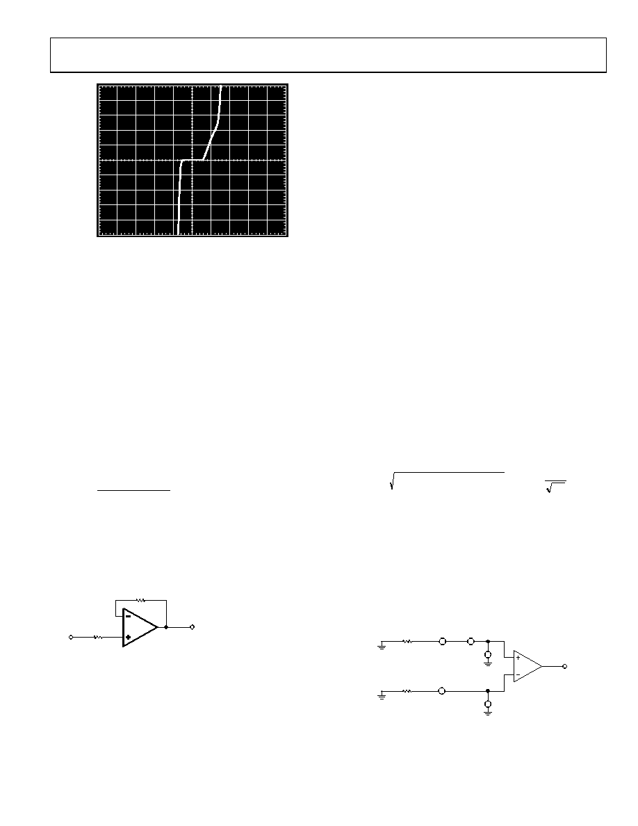
Figure 46. Input Overvoltage I-V Characteristics of the OP284
As shown in Figure 46, internal p-n junctions to the OP284
energize and permit current flow from the inputs to the supplies
when the input is 1.8 V more positive and 0.6 V more negative
than the respective supply rails. As illustrated in the simplified
equivalent circuit shown in Figure 44, the OP284 does not have
any internal current limiting resistors; thus, fault currents can
quickly rise to damaging levels.
This input current is not inherently damaging to the device,
provided that it is limited to 5 mA or less. For the OP284, once
the input exceeds the negative supply by 0.6 V, the input current
quickly exceeds 5 mA. If this condition continues to exist, an
external series resistor should be added at the expense of addi-
tional thermal noise. Figure 47 illustrates a typical noninverting
configuration for an overvoltage-protected amplifier where the
series resistance, RS, is chosen such that
(
)
mA
5
SUPPLY
MAX
IN
S
V
R
=
For example, a 1 kΩ resistor protects the OP284 against input
signals up to 5 V above and below the supplies. For other configu-
rations where both inputs are used, each input should be protected
against abuse with a series resistor. Again, to ensure optimum
dc and ac performance, it is recommended that source impedance
levels be balanced.
R1
R2
VIN
VOUT
1/2
OP284
00293-
047
Figure 47. Resistance in Series with Input Limits Overvoltage Currents
to Safe Values
OUTPUT PHASE REVERSAL
Some operational amplifiers designed for single-supply operation
exhibit an output voltage phase reversal when their inputs are
driven beyond their useful common-mode range. Typically, for
single-supply bipolar op amps, the negative supply determines
the lower limit of their common-mode range. With these devices,
external clamping diodes, with the anode connected to ground
and the cathode to the inputs, prevent input signal excursions
from exceeding the negative supply of the device (that is, GND),
preventing a condition that causes the output voltage to change
phase. JFET-input amplifiers can also exhibit phase reversal;
and, if so, a series input resistor is usually required to prevent it.
The OP284 is free from reasonable input voltage range restrictions,
provided that input voltages no greater than the supply voltages
are applied. Although device output does not change phase, large
currents can flow through the input protection diodes, as shown
in Figure 46. Therefore, the technique recommended in the Input
Overvoltage Protection section should be applied to those appli-
cations where the likelihood of input voltages exceeding the
supply voltages is high.
DESIGNING LOW NOISE CIRCUITS IN SINGLE-
SUPPLY APPLICATIONS
In single-supply applications, devices like the OP284 extend the
dynamic range of the application through the use of rail-to-rail
operation. In fact, the OPx84 family is the first of its kind to
combine single-supply, rail-to-rail operation, and low noise in
one device. It is the first device in the industry to exhibit an input
noise voltage spectral density of less than 4 nV/√Hz at 1 kHz.
It was also designed specifically for low-noise, single-supply
applications, and as such, some discussion on circuit noise
concepts in single-supply applications is appropriate.
Referring to the op amp noise model circuit configuration
illustrated in Figure 48, the expression for an amplifier’s total
equivalent input noise voltage for a source resistance level, RS,
is given by
[
]
2
)
(
)
(
)
(
2
nOA
S
nOA
nR
nT
e
R
i
+
×
+
=
, units in
Hz
V
where:
RS = 2R is the effective, or equivalent, circuit source resistance.
(enR)2 is the source resistance thermal noise voltage power (4kTR).
k is the Boltzmann’s constant = 1.38 × 10⁻²³ J/K.
T is the ambient temperature in Kelvins of the circuit = 273.15 +
TA (°C).
(inOA)2 is the op amp equivalent input noise current spectral power
(1 Hz bandwidth).
(enOA)2 is the op amp equivalent input noise voltage spectral power
(1 Hz bandwidth).
enR
enOA
inOA
R
NOISELESS
R
NOISELESS
00293-
048
IDEAL
NOISELESS
OP AMP
RS = 2R
Figure 48. Op Amp Noise Circuit Model Used to Determine Total Circuit
Equivalent Input Noise Voltage and Noise Figure
相关PDF资料 |
PDF描述 |
|---|---|
| ADA4817-2ACPZ-R7 | IC OPAMP VF 410MHZ DUAL 16LFCSP |
| LT1113CN8#PBF | IC PREC OP-AMP JFET DUAL 8-DIP |
| LTC1152CN8#PBF | IC OPAMP 0-DRFT R-R IN/OUT 8DIP |
| OP293FSZ | IC OPAMP GP 35KHZ DUAL 8SOIC |
| 929500-01-14 | CONN HEADER .100 SNGL R/A 14POS |
相关代理商/技术参数 |
参数描述 |
|---|---|
| OP184ESZ | 制造商:Analog Devices 功能描述:Operational Amplifier (Op-Amp) IC 制造商:Analog Devices 功能描述:IC, OP-AMP, 4.25MHZ, 4V/ us, SOIC-8 |
| OP184ESZ-REEL | 功能描述:IC OPAMP GP R-R 4.25MHZ LN 8SOIC RoHS:是 类别:集成电路 (IC) >> Linear - Amplifiers - Instrumentation 系列:- 产品培训模块:Lead (SnPb) Finish for COTS Obsolescence Mitigation Program 标准包装:1 系列:- 放大器类型:电流检测 电路数:1 输出类型:- 转换速率:- 增益带宽积:125kHz -3db带宽:- 电流 - 输入偏压:- 电压 - 输入偏移:100µV 电流 - 电源:1.1µA 电流 - 输出 / 通道:- 电压 - 电源,单路/双路(±):- 工作温度:-40°C ~ 85°C 安装类型:表面贴装 封装/外壳:4-WFBGA,CSPBGA 供应商设备封装:4-UCSP(2x2) 包装:剪切带 (CT) 其它名称:MAX9634WERS+TCT |
| OP184ESZ-REEL7 | 功能描述:IC OPAMP GP R-R 4.25MHZ LN 8SOIC RoHS:是 类别:集成电路 (IC) >> Linear - Amplifiers - Instrumentation 系列:- 标准包装:100 系列:- 放大器类型:通用 电路数:1 输出类型:- 转换速率:0.2 V/µs 增益带宽积:- -3db带宽:- 电流 - 输入偏压:100pA 电压 - 输入偏移:30µV 电流 - 电源:380µA 电流 - 输出 / 通道:- 电压 - 电源,单路/双路(±):±2 V ~ 18 V 工作温度:0°C ~ 70°C 安装类型:表面贴装 封装/外壳:8-SOIC(0.154",3.90mm 宽) 供应商设备封装:8-SO 包装:管件 |
| OP184FP | 制造商:AD 制造商全称:Analog Devices 功能描述:Precision Rail-to-Rail Input & Output Operational Amplifiers |
| OP184FS | 功能描述:IC OPAMP GP R-R 4.25MHZ LN 8SOIC RoHS:否 类别:集成电路 (IC) >> Linear - Amplifiers - Instrumentation 系列:- 标准包装:1 系列:- 放大器类型:通用 电路数:4 输出类型:满摆幅 转换速率:0.028 V/µs 增益带宽积:105kHz -3db带宽:- 电流 - 输入偏压:3nA 电压 - 输入偏移:100µV 电流 - 电源:3.3µA 电流 - 输出 / 通道:12mA 电压 - 电源,单路/双路(±):2.7 V ~ 12 V,±1.35 V ~ 6 V 工作温度:-40°C ~ 85°C 安装类型:表面贴装 封装/外壳:14-TSSOP(0.173",4.40mm 宽) 供应商设备封装:14-TSSOP 包装:剪切带 (CT) 其它名称:OP481GRUZ-REELCT |
发布紧急采购,3分钟左右您将得到回复。