- 您现在的位置:买卖IC网 > PDF目录5272 > OP184FS-REEL7 (Analog Devices Inc)IC OPAMP GP R-R 4.25MHZ LN 8SOIC PDF资料下载
参数资料
| 型号: | OP184FS-REEL7 |
| 厂商: | Analog Devices Inc |
| 文件页数: | 13/24页 |
| 文件大小: | 0K |
| 描述: | IC OPAMP GP R-R 4.25MHZ LN 8SOIC |
| 设计资源: | Variable Gain Noninverting Amplifier Using AD5292 and OP184 (CN0112) Variable Gain Inverting Amplifier Using AD5292 and OP184 (CN0113) Programmable High Voltage Source with Boosted Output Current Using AD5292, OP184, and MOSFETs (CN0115) Low-Noise Microwave fractional-N PLL using active loop filter and RF prescaler (CN0174) |
| 标准包装: | 1,000 |
| 放大器类型: | 通用 |
| 电路数: | 1 |
| 输出类型: | 满摆幅 |
| 转换速率: | 4 V/µs |
| 增益带宽积: | 4.25MHz |
| 电流 - 输入偏压: | 80nA |
| 电压 - 输入偏移: | 175µV |
| 电流 - 电源: | 2.25mA |
| 电流 - 输出 / 通道: | 10mA |
| 电压 - 电源,单路/双路(±): | 3 V ~ 36 V,±1.5 V ~ 18 V |
| 工作温度: | -40°C ~ 125°C |
| 安装类型: | 表面贴装 |
| 封装/外壳: | 8-SOIC(0.154",3.90mm 宽) |
| 供应商设备封装: | 8-SO |
| 包装: | 带卷 (TR) |
OP184/OP284/OP484
Rev. J | Page 20 of 24
Obviously, it is desirable to keep this comparison voltage small
because it becomes a significant portion of the overall dropout
voltage. Here, the 20 mV reference is higher than the typical
offset of the OP284 but is still reasonably low as a percentage
of VOUT (<0.5%). In adapting the limiter for other ILIMIT levels,
Sense Resistor RS should be adjusted along with R7 to R8, to
maintain this threshold voltage between 20 mV and 50 mV.
Performance of the circuit is excellent. For the 4.5 V output
version, the measured dc output change for a 225 mA load
change was on the order of a few microvolts, while the dropout
voltage at this same current level was about 30 mV. The current
limit, as shown in Figure 58, is 400 mA, allowing the circuit to
be used at levels up to 300 mA or more. While the Q1 device can
actually support currents of several amperes, a practical current
rating takes into account the 2.5 W, 25°C dissipation of the
8-lead SOIC device. Because a short-circuit current of 400 mA
at an input level of 5 V causes a 2 W dissipation in Q1, other input
conditions must be considered carefully in terms of potential
overheating of Q1. Of course, if higher powered devices are used
for Q1, this circuit can support outputs of tens of amperes as
well as the higher VOUT levels already noted.
The circuit shown can either be used as a standard low dropout
regulator, or it can be used with on/off control. By driving Pin 3
of U2 with the optional logic control signal, VC, the output is
switched between on and off. Note that when the output is off
in this circuit, it is still active (that is, not an open circuit). This
is because the off state simply reduces the voltage input to R1,
leaving the U1A/U1B amplifiers and Q1 still active.
When the on/off control is used, Resistor R10 should be used
with U2 to speed on/off switching and to allow the output of the
circuit to settle to a nominal zero voltage. Component D3 and
Component R11 also aid in speeding up the on/off transition by
providing a dynamic discharge path for C2. Off/on transition
time is less than 1 ms, while the on/off transition is longer, but
less than 10 ms.
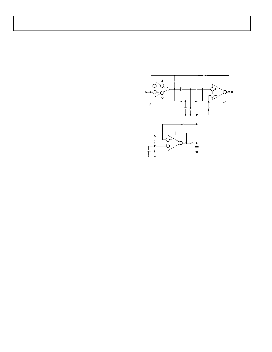
3 V, 50 HZ/60 HZ ACTIVE NOTCH FILTER WITH
FALSE GROUND
To process signals in a single-supply system, it is often best to use
a false ground biasing scheme. A circuit that uses this approach is
shown in Figure 59. In this circuit, a false ground circuit biases
an active notch filter used to reject 50 Hz/60 Hz power line
interference in portable patient monitoring equipment.
Notch filters are commonly used to reject power line frequency
interference that often obscures low frequency physiological
signals, such as heart rates, blood pressure readings, EEGs, and
EKGs. This notch filter effectively squelches 60 Hz pickup at a
Filter Q of 0.75. Substituting 3.16 kΩ resistors for the 2.67 kΩ
resistor in the twin-T section (R1 through R5) configures the
active filter to reject 50 Hz interference.
00293-
059
R2
2.67k
R6
10k
R7
1k
R8
1k
R11
10k
R9
20k
R12
150
R10
20k
1
3
5
6
7
11
2
3V
VO
VIN
A2
A1
8
A3
4
10
9
3V
A1, A2, A3 = OP484
Q = 0.75
NOTE: FOR 50Hz APPLICATIONS
CHANGE R1, R2, R3, AND R4 TO 3.1k
AND R5 TO 1.58k
(3.16k ÷ 2).
R3
2.67k
R1
2.67k
R4
2.67k
R5
1.33k
(2.68k
÷ 2)
C3
2F
(1F × 2)
C5
0.03F
C1
1F
C2
1F
C4
1F
C6
1F
1.5V
Figure 59. A 3 V Single-Supply, 50Hz to 60 Hz Active Notch Filter
with False Ground
Amplifier A3 is the heart of the false ground bias circuit. It buffers
the voltage developed at R9 and R10 and is the reference for the
active notch filter. Because the OP484 exhibits a rail-to-rail input
common-mode range, R9 and R10 are chosen to split the 3 V
supply symmetrically. An in-the-loop compensation scheme is
used around the OP484 that allows the op amp to drive C6, a
1 μF capacitor, without oscillation. C6 maintains a low impedance
ac ground over the operating frequency range of the filter.
The filter section uses an OP484 in a Twin-T configuration whose
frequency selectivity is very sensitive to the relative matching of
the capacitors and resistors in the twin-T section. Mylar is the
material of choice for the capacitors, and the relative matching
of the capacitors and resistors determines the pass band symmetry
of the filter. Using 1% resistors and 5% capacitors produces satis-
factory results.
相关PDF资料 |
PDF描述 |
|---|---|
| 0031.8552 | FUSE 80MA 250VAC 5X20 FAST |
| 0031.8551 | FUSE 63MA 250VAC 5X20 FAST |
| EL5260IY-T13 | IC AMP CFA DUAL 200MHZ 10-MSOP |
| EL5257IY-T13 | IC AMP VFA DUAL 600MHZ 8-MSOP |
| 0031.8555 | FUSE 160MA 250VAC 5X20 FAST |
相关代理商/技术参数 |
参数描述 |
|---|---|
| OP184FSZ | 功能描述:IC OPAMP GP R-R 4.25MHZ LN 8SOIC RoHS:是 类别:集成电路 (IC) >> Linear - Amplifiers - Instrumentation 系列:- 标准包装:1 系列:- 放大器类型:通用 电路数:4 输出类型:满摆幅 转换速率:0.028 V/µs 增益带宽积:105kHz -3db带宽:- 电流 - 输入偏压:3nA 电压 - 输入偏移:100µV 电流 - 电源:3.3µA 电流 - 输出 / 通道:12mA 电压 - 电源,单路/双路(±):2.7 V ~ 12 V,±1.35 V ~ 6 V 工作温度:-40°C ~ 85°C 安装类型:表面贴装 封装/外壳:14-TSSOP(0.173",4.40mm 宽) 供应商设备封装:14-TSSOP 包装:剪切带 (CT) 其它名称:OP481GRUZ-REELCT |
| OP184FSZ | 制造商:Analog Devices 功能描述:Operational Amplifier (Op-Amp) IC |
| OP184FSZ-REEL | 功能描述:IC OPAMP GP R-R 4.25MHZ LN 8SOIC RoHS:是 类别:集成电路 (IC) >> Linear - Amplifiers - Instrumentation 系列:- 标准包装:1,000 系列:- 放大器类型:电压反馈 电路数:4 输出类型:满摆幅 转换速率:33 V/µs 增益带宽积:20MHz -3db带宽:30MHz 电流 - 输入偏压:2nA 电压 - 输入偏移:3000µV 电流 - 电源:2.5mA 电流 - 输出 / 通道:30mA 电压 - 电源,单路/双路(±):4.5 V ~ 16.5 V,±2.25 V ~ 8.25 V 工作温度:-40°C ~ 85°C 安装类型:表面贴装 封装/外壳:14-SOIC(0.154",3.90mm 宽) 供应商设备封装:14-SOIC 包装:带卷 (TR) |
| OP184FSZ-REEL7 | 功能描述:IC OPAMP GP R-R 4.25MHZ LN 8SOIC RoHS:是 类别:集成电路 (IC) >> Linear - Amplifiers - Instrumentation 系列:- 产品培训模块:Differential Circuit Design Techniques for Communication Applications 标准包装:1 系列:- 放大器类型:RF/IF 差分 电路数:1 输出类型:差分 转换速率:9800 V/µs 增益带宽积:- -3db带宽:2.9GHz 电流 - 输入偏压:3µA 电压 - 输入偏移:- 电流 - 电源:40mA 电流 - 输出 / 通道:- 电压 - 电源,单路/双路(±):3 V ~ 3.6 V 工作温度:-40°C ~ 85°C 安装类型:表面贴装 封装/外壳:16-VQFN 裸露焊盘,CSP 供应商设备封装:16-LFCSP-VQ 包装:剪切带 (CT) 产品目录页面:551 (CN2011-ZH PDF) 其它名称:ADL5561ACPZ-R7CT |
| OP186 | 制造商:AD 制造商全称:Analog Devices 功能描述:5 uA, Rail-to-Rail Output Operational Amplifier |
发布紧急采购,3分钟左右您将得到回复。