- 您现在的位置:买卖IC网 > PDF目录5272 > OP184FS-REEL7 (Analog Devices Inc)IC OPAMP GP R-R 4.25MHZ LN 8SOIC PDF资料下载
参数资料
| 型号: | OP184FS-REEL7 |
| 厂商: | Analog Devices Inc |
| 文件页数: | 9/24页 |
| 文件大小: | 0K |
| 描述: | IC OPAMP GP R-R 4.25MHZ LN 8SOIC |
| 设计资源: | Variable Gain Noninverting Amplifier Using AD5292 and OP184 (CN0112) Variable Gain Inverting Amplifier Using AD5292 and OP184 (CN0113) Programmable High Voltage Source with Boosted Output Current Using AD5292, OP184, and MOSFETs (CN0115) Low-Noise Microwave fractional-N PLL using active loop filter and RF prescaler (CN0174) |
| 标准包装: | 1,000 |
| 放大器类型: | 通用 |
| 电路数: | 1 |
| 输出类型: | 满摆幅 |
| 转换速率: | 4 V/µs |
| 增益带宽积: | 4.25MHz |
| 电流 - 输入偏压: | 80nA |
| 电压 - 输入偏移: | 175µV |
| 电流 - 电源: | 2.25mA |
| 电流 - 输出 / 通道: | 10mA |
| 电压 - 电源,单路/双路(±): | 3 V ~ 36 V,±1.5 V ~ 18 V |
| 工作温度: | -40°C ~ 125°C |
| 安装类型: | 表面贴装 |
| 封装/外壳: | 8-SOIC(0.154",3.90mm 宽) |
| 供应商设备封装: | 8-SO |
| 包装: | 带卷 (TR) |
OP184/OP284/OP484
Rev. J | Page 17 of 24
Resistor networks should be used in this circuit for R2 and R3
because they exhibit the necessary relative tolerance matching for
good performance. Matched networks also exhibit tight relative
resistor temperature coefficients for good circuit temperature
stability. Trimming Potentiometer P1 is used for optimum dc
CMR adjustment, and C1 is used to optimize ac CMR. With the
circuit values as shown, Circuit CMR is better than 80 dB over the
frequency range of 20 Hz to 20 kHz. Circuit referred-to-input
(RTI) noise in the 0.1 Hz to 10 Hz band is an impressively low
0.45 μV p-p. Resistor RP1 and Resistor RP2 serve to protect the
OP284 inputs against input overvoltage abuse. Capacitor C2 can
be included to the limit circuit bandwidth and, therefore, wide
bandwidth noise in sensitive applications. The value of this
capacitor should be adjusted, depending on the required closed-
loop bandwidth of the circuit. The R4 to C2 time constant creates
a pole at a frequency equal to
( )
2
4
2
1
3
C
R
dB
f
π
=
2.5 V REFERENCE FROM A 3 V SUPPLY
In many single-supply applications, the need for a 2.5 V reference
often arises. Many commercially available monolithic 2.5 V
references require at least a minimum operating supply of 4 V.
The problem is exacerbated when the minimum operating
supply voltage is 3 V. The circuit illustrated in Figure 53 is an
example of a 2.5 V reference that operates from a single 3 V
supply. The circuit takes advantage of the OP284 rail-to-rail
input/output voltage ranges to amplify an AD589 1.235 V
output to 2.5 V.
00293-
052
VOUT
5
6
7
3V
A1, A2 = 1/2 OP284
GAIN = 1 +
R4
R3
SET R2 = R3
R1 + P1 = R4
8
4
C2
RP1
1k
RP2
1k
R1
9.53k
R2
1.1k
R3
1.1k
R4
10k
P1
500
3
2
1
VIN
A1
+
–
A2
C1
AC CMRR
TRIM
5pF TO 40pF
Figure 52. Single Supply, 3 V Low Noise Instrumentation Amplifier
The low TCVOS of the OP284 at 1.5 μV/°C helps maintain an
output voltage temperature coefficient that is dominated by
the temperature coefficients of R2 and R3. In this circuit with
100 ppm/°C TCR resistors, the output voltage exhibits a tempera-
ture coefficient of 200 ppm/°C. Lower tempco resistors are
recommended for more accurate performance over temperature.
One measure of the performance of a voltage reference is its
capacity to recover from sudden changes in load current. While
sourcing a steady-state load current of 1 mA, this circuit recovers
to 0.01% of the programmed output voltage in 1.5 μs for a total
change in load current of ±1 mA.
00293-
053
2.5VREF
3
2
1
3V
8
4
R3
100k
R2
100k
P1
5k
R1
17.4k
3V
0.1F
AD589
1/2
OP284
+
–
RESISTORS = 1%, 100ppm/°C
POTENTIOMETER = 10 TURN, 100ppm/°C
Figure 53. 2.5 V Reference That Operates on a Single 3 V Supply
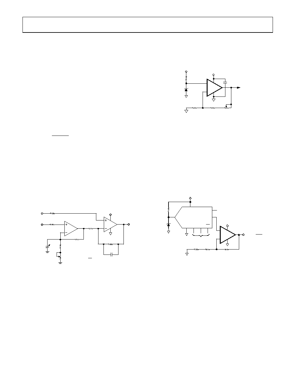
5 V ONLY, 12-BIT DAC SWINGS RAIL-TO-RAIL
The OP284 is ideal for use with a CMOS DAC to generate a
digitally controlled voltage with a wide output range. Figure 54
shows a DAC8043 used in conjunction with the AD589 to gen-
erate a voltage output from 0 V to 1.23 V. The DAC is actually
operating in voltage switching mode, where the reference is
connected to the current output, IOUT, and the output voltage is
taken from the VREF pin. This topology is inherently noninverting,
as opposed to the classic current output mode, which is inverting
and not usable in single-supply applications.
3
2
1
5V
8
4
R3
232
1%
R2
32.4
1%
R1
17.8k
R4
100k
1%
AD589
GND CLK SR1
LD
VREF
RRB
VDD
IOUT
1.23V
4
8
2
1
3
DAC8043
DIGITAL
CONTROL
7
6
5
1/2
OP284
VOUT =
D
4096
(5V)
00293-
054
Figure 54. 5 V Only, 12-Bit DAC Swings Rail-to-Rail
In this application, the OP284 serves two functions. First, it
buffers the high output impedance of the DAC VREF pin, which
is on the order of 10 kΩ. The op amp provides a low impedance
output to drive any following circuitry.
Second, the op amp amplifies the output signal to provide a rail-
to-rail output swing. In this particular case, the gain is set to 4.1
so that the circuit generates a 5 V output when the DAC output
is at full scale. If other output voltage ranges are needed, such as
0 V ≤ VOUT ≤ 4.095 V, the gain can be easily changed by adjusting
the values of R2 and R3.
相关PDF资料 |
PDF描述 |
|---|---|
| 0031.8552 | FUSE 80MA 250VAC 5X20 FAST |
| 0031.8551 | FUSE 63MA 250VAC 5X20 FAST |
| EL5260IY-T13 | IC AMP CFA DUAL 200MHZ 10-MSOP |
| EL5257IY-T13 | IC AMP VFA DUAL 600MHZ 8-MSOP |
| 0031.8555 | FUSE 160MA 250VAC 5X20 FAST |
相关代理商/技术参数 |
参数描述 |
|---|---|
| OP184FSZ | 功能描述:IC OPAMP GP R-R 4.25MHZ LN 8SOIC RoHS:是 类别:集成电路 (IC) >> Linear - Amplifiers - Instrumentation 系列:- 标准包装:1 系列:- 放大器类型:通用 电路数:4 输出类型:满摆幅 转换速率:0.028 V/µs 增益带宽积:105kHz -3db带宽:- 电流 - 输入偏压:3nA 电压 - 输入偏移:100µV 电流 - 电源:3.3µA 电流 - 输出 / 通道:12mA 电压 - 电源,单路/双路(±):2.7 V ~ 12 V,±1.35 V ~ 6 V 工作温度:-40°C ~ 85°C 安装类型:表面贴装 封装/外壳:14-TSSOP(0.173",4.40mm 宽) 供应商设备封装:14-TSSOP 包装:剪切带 (CT) 其它名称:OP481GRUZ-REELCT |
| OP184FSZ | 制造商:Analog Devices 功能描述:Operational Amplifier (Op-Amp) IC |
| OP184FSZ-REEL | 功能描述:IC OPAMP GP R-R 4.25MHZ LN 8SOIC RoHS:是 类别:集成电路 (IC) >> Linear - Amplifiers - Instrumentation 系列:- 标准包装:1,000 系列:- 放大器类型:电压反馈 电路数:4 输出类型:满摆幅 转换速率:33 V/µs 增益带宽积:20MHz -3db带宽:30MHz 电流 - 输入偏压:2nA 电压 - 输入偏移:3000µV 电流 - 电源:2.5mA 电流 - 输出 / 通道:30mA 电压 - 电源,单路/双路(±):4.5 V ~ 16.5 V,±2.25 V ~ 8.25 V 工作温度:-40°C ~ 85°C 安装类型:表面贴装 封装/外壳:14-SOIC(0.154",3.90mm 宽) 供应商设备封装:14-SOIC 包装:带卷 (TR) |
| OP184FSZ-REEL7 | 功能描述:IC OPAMP GP R-R 4.25MHZ LN 8SOIC RoHS:是 类别:集成电路 (IC) >> Linear - Amplifiers - Instrumentation 系列:- 产品培训模块:Differential Circuit Design Techniques for Communication Applications 标准包装:1 系列:- 放大器类型:RF/IF 差分 电路数:1 输出类型:差分 转换速率:9800 V/µs 增益带宽积:- -3db带宽:2.9GHz 电流 - 输入偏压:3µA 电压 - 输入偏移:- 电流 - 电源:40mA 电流 - 输出 / 通道:- 电压 - 电源,单路/双路(±):3 V ~ 3.6 V 工作温度:-40°C ~ 85°C 安装类型:表面贴装 封装/外壳:16-VQFN 裸露焊盘,CSP 供应商设备封装:16-LFCSP-VQ 包装:剪切带 (CT) 产品目录页面:551 (CN2011-ZH PDF) 其它名称:ADL5561ACPZ-R7CT |
| OP186 | 制造商:AD 制造商全称:Analog Devices 功能描述:5 uA, Rail-to-Rail Output Operational Amplifier |
发布紧急采购,3分钟左右您将得到回复。