参数资料
| 型号: | OP262GS |
| 厂商: | Analog Devices Inc |
| 文件页数: | 7/20页 |
| 文件大小: | 0K |
| 描述: | IC OPAMP GP R-R 15MHZ DUAL 8SOIC |
| 标准包装: | 98 |
| 放大器类型: | 通用 |
| 电路数: | 2 |
| 输出类型: | 满摆幅 |
| 转换速率: | 13 V/µs |
| 增益带宽积: | 15MHz |
| 电流 - 输入偏压: | 260nA |
| 电压 - 输入偏移: | 25µV |
| 电流 - 电源: | 550µA |
| 电流 - 输出 / 通道: | 30mA |
| 电压 - 电源,单路/双路(±): | 2.7 V ~ 12 V,±1.35 V ~ 6 V |
| 工作温度: | -40°C ~ 125°C |
| 安装类型: | 表面贴装 |
| 封装/外壳: | 8-SOIC(0.154",3.90mm 宽) |
| 供应商设备封装: | 8-SO |
| 包装: | 管件 |
Data Sheet
OP162/OP262/OP462
Rev. H | Page 15 of 20
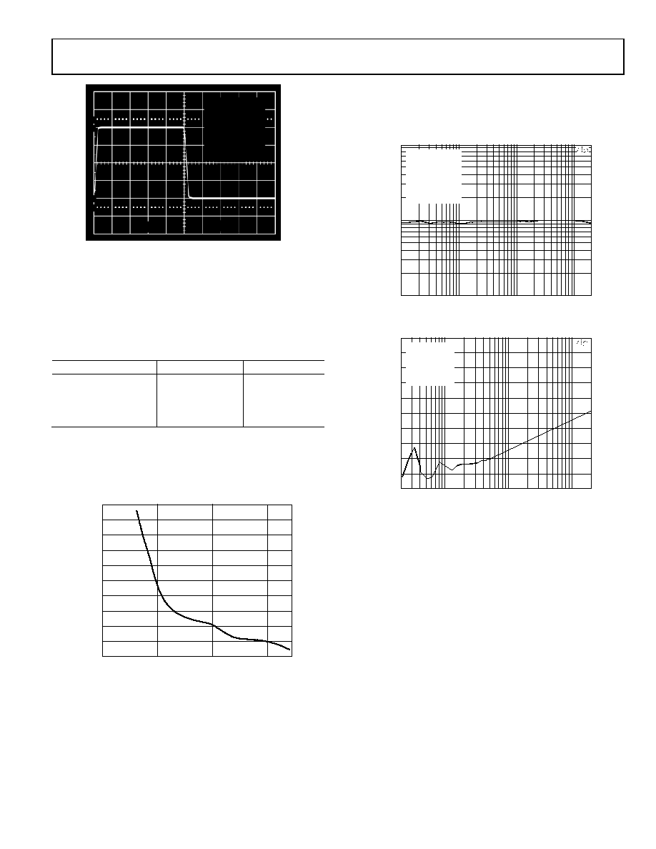
Figure 39. A Photo of a Nice Square Wave at the Output
The network operates in parallel with the load capacitor, CL,
and provides compensation for the added phase lag. The actual
values of the network resistor and capacitor are empirically
determined to minimize overshoot and maximize unity-gain
bandwidth. Table 6 shows a few sample snubber networks for
large load capacitors.
Table 6. Snubber Networks for Large Capacitive Loads
CLOAD
RX
CX
< 300 pF
140 Ω
10 nF
500 pF
100 Ω
10 nF
1 nF
80 Ω
10 nF
10 Ω
47 nF
Higher load capacitance will reduce the unity-gain bandwidth
of the device. Figure 40 shows unity-gain bandwidth vs.
capacitive load. The snubber network does not provide any
increase in bandwidth, but it substantially reduces ringing and
overshoot, as shown between Figure 38 and Figure 39.
Figure 40. Unity-Gain Bandwidth vs. CLOAD
TOTAL HARMONIC DISTORTION AND CROSSTALK
The OPx62 device family offers low total harmonic distortion
making it an excellent choice for audio applications. Figure 41
shows a graph of THD plus noise figures at 0.001% for the
OP462.
Figure 42 shows the worst case crosstalk between two amplifiers
in the OP462. A 1 V rms signal is applied to one amplifier while
measuring the output of an adjacent amplifier. Both amplifiers
are configured for unity gain and supplied with ±2.5 V.
Figure 41. THD + N vs. Frequency
Figure 42. Crosstalk vs. Frequency
PCB LAYOUT CONSIDERATIONS
Because the OP162/OP262/OP462 can provide gains at high
frequency, careful attention to board layout and component
selection is recommended. As with any high speed application,
a good ground plane is essential to achieve the optimum
performance. This can significantly reduce the undesirable
effects of ground loops and I × R losses by providing a low
impedance reference point. Best results are obtained with a
multilayer board design with one layer assigned to ground
plane.
Use chip capacitors for supply bypassing, with one end of the
capacitor connected to the ground plane and the other end
connected within 1/8 inch of each power pin. An additional
large tantalum electrolytic capacitor (4.7 F to 10 F) should be
connected in parallel. This capacitor provides current for fast,
large-signal changes at the device’s output; therefore, it does not
need to be placed as close to the supply pins.
00288-
042
10
0%
100
90
50mV
1s
VS = 5V
AV = 1
CL = 300pF
RL = 10k
WITH SNUBBER:
RX = 140
CX = 10nF
CLOAD
BANDWIDTH
(MHz)
10
7
8
9
5
6
4
3
2
1
0
10pF
100pF
1nF
10nF
00288-043
FREQUENCY (Hz)
THD+N
(%)
0.010
0.001
0.0001
20
100
1k
10k
20k
00288-044
VS = ±2.5V
AV = 1
VIN = 1.0V rms
RL = 10k
BANDWIDTH:
<10Hz TO 22kHz
FREQUENCY (Hz)
XTALK
(dBV)
–40
–90
–80
–70
–60
–50
–140
–130
–120
–110
–100
20
100
1k
10k
20k
00288-045
AV = 1
VIN = 1.0V rms
(0dBV)
RL = 10k
VS = ±2.5V
相关PDF资料 |
PDF描述 |
|---|---|
| 52929-3 | CONN SPADE SPRING 16-22 AWG #6 |
| 2036-15-A | GAS DISCHARGE TUBE MINI 3 POLE |
| 2-32562-3 | CONN SPADE FLANGE 22-16AWG #8 |
| BK1/S506-8-R | FUSE 8A 250V TLAG GLS 5X20 IEC |
| BK/S506-V-500-R | FUSE 500MA 250V T-LAG GLASS S506 |
相关代理商/技术参数 |
参数描述 |
|---|---|
| OP262GS | 制造商:Analog Devices 功能描述:IC SM OP-AMP DUAL 15MHZ RRO/P ((NS)) |
| OP262GS-REEL | 功能描述:IC OPAMP GP R-R 15MHZ DUAL 8SOIC RoHS:否 类别:集成电路 (IC) >> Linear - Amplifiers - Instrumentation 系列:- 产品培训模块:Lead (SnPb) Finish for COTS Obsolescence Mitigation Program 标准包装:1 系列:- 放大器类型:电流检测 电路数:1 输出类型:- 转换速率:- 增益带宽积:125kHz -3db带宽:- 电流 - 输入偏压:- 电压 - 输入偏移:100µV 电流 - 电源:1.1µA 电流 - 输出 / 通道:- 电压 - 电源,单路/双路(±):- 工作温度:-40°C ~ 85°C 安装类型:表面贴装 封装/外壳:4-WFBGA,CSPBGA 供应商设备封装:4-UCSP(2x2) 包装:剪切带 (CT) 其它名称:MAX9634WERS+TCT |
| OP262GS-REEL7 | 功能描述:IC OPAMP GP R-R 15MHZ DUAL 8SOIC RoHS:否 类别:集成电路 (IC) >> Linear - Amplifiers - Instrumentation 系列:- 标准包装:100 系列:- 放大器类型:通用 电路数:1 输出类型:- 转换速率:0.2 V/µs 增益带宽积:- -3db带宽:- 电流 - 输入偏压:100pA 电压 - 输入偏移:30µV 电流 - 电源:380µA 电流 - 输出 / 通道:- 电压 - 电源,单路/双路(±):±2 V ~ 18 V 工作温度:0°C ~ 70°C 安装类型:表面贴装 封装/外壳:8-SOIC(0.154",3.90mm 宽) 供应商设备封装:8-SO 包装:管件 |
| OP262GSZ | 功能描述:IC OPAMP GP R-R 15MHZ DUAL 8SOIC RoHS:是 类别:集成电路 (IC) >> Linear - Amplifiers - Instrumentation 系列:- 标准包装:2,500 系列:- 放大器类型:通用 电路数:4 输出类型:- 转换速率:0.6 V/µs 增益带宽积:1MHz -3db带宽:- 电流 - 输入偏压:45nA 电压 - 输入偏移:2000µV 电流 - 电源:1.4mA 电流 - 输出 / 通道:40mA 电压 - 电源,单路/双路(±):3 V ~ 32 V,±1.5 V ~ 16 V 工作温度:0°C ~ 70°C 安装类型:表面贴装 封装/外壳:14-TSSOP(0.173",4.40mm 宽) 供应商设备封装:14-TSSOP 包装:带卷 (TR) 其它名称:LM324ADTBR2G-NDLM324ADTBR2GOSTR |
| OP262GSZ-REEL | 功能描述:IC OPAMP GP R-R 15MHZ DUAL 8SOIC RoHS:是 类别:集成电路 (IC) >> Linear - Amplifiers - Instrumentation 系列:- 标准包装:50 系列:LinCMOS™ 放大器类型:通用 电路数:4 输出类型:- 转换速率:0.05 V/µs 增益带宽积:110kHz -3db带宽:- 电流 - 输入偏压:0.7pA 电压 - 输入偏移:210µV 电流 - 电源:57µA 电流 - 输出 / 通道:30mA 电压 - 电源,单路/双路(±):3 V ~ 16 V,±1.5 V ~ 8 V 工作温度:-40°C ~ 85°C 安装类型:表面贴装 封装/外壳:14-SOIC(0.154",3.90mm 宽) 供应商设备封装:14-SOIC 包装:管件 产品目录页面:865 (CN2011-ZH PDF) 其它名称:296-1834296-1834-5 |
发布紧急采购,3分钟左右您将得到回复。