参数资料
| 型号: | OP262GS |
| 厂商: | Analog Devices Inc |
| 文件页数: | 8/20页 |
| 文件大小: | 0K |
| 描述: | IC OPAMP GP R-R 15MHZ DUAL 8SOIC |
| 标准包装: | 98 |
| 放大器类型: | 通用 |
| 电路数: | 2 |
| 输出类型: | 满摆幅 |
| 转换速率: | 13 V/µs |
| 增益带宽积: | 15MHz |
| 电流 - 输入偏压: | 260nA |
| 电压 - 输入偏移: | 25µV |
| 电流 - 电源: | 550µA |
| 电流 - 输出 / 通道: | 30mA |
| 电压 - 电源,单路/双路(±): | 2.7 V ~ 12 V,±1.35 V ~ 6 V |
| 工作温度: | -40°C ~ 125°C |
| 安装类型: | 表面贴装 |
| 封装/外壳: | 8-SOIC(0.154",3.90mm 宽) |
| 供应商设备封装: | 8-SO |
| 包装: | 管件 |
OP162/OP262/OP462
Data Sheet
Rev. H | Page 16 of 20
APPLICATIONS CIRCUITS
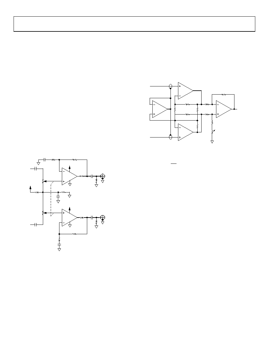
SINGLE-SUPPLY STEREO HEADPHONE DRIVER
Figure 43 shows a stereo headphone output amplifier that can
operate from a single 5 V supply. The reference voltage is
derived by dividing the supply voltage down with two 100 k
resistors. A 10 F capacitor prevents power supply noise from
contaminating the audio signal and establishes an ac ground for
the volume control potentiometers.
The audio signal is ac-coupled to each noninverting input
through a 10 F capacitor. The gain of the amplifier is con-
trolled by the feedback resistors and is (R2/R1) + 1. For this
example, the gain is 6. By removing R1, the amplifier would
have unity gain. To short-circuit protect the output of the
device, a 169 resistor is placed at the output in the feedback
network. This prevents any damage to the device if the head-
phone output becomes shorted. A 270 F capacitor is used at
the output to couple the amplifier to the headphone. This value
is much larger than that used for the input because of the low
impedance of headphones, which can range from 32 to 600
or more.
Figure 43. Headphone Output Amplifier
INSTRUMENTATION AMPLIFIER
Because of their high speed, low offset voltages, and low noise
characteristics, the OP162/OP262/OP462 can be used in a wide
variety of high speed applications, including precision instru-
mentation amplifiers. Figure 44 shows an example of such an
application.
Figure 44. High Speed Instrumentation Amplifier
The differential gain of the circuit is determined by RG, where
G
DIFF
R
A
2
1+
=
with the RG resistor value in k. Removing RG sets the circuit
gain to unity.
The fourth op amp, OP462-D, is optional and is used to
improve CMRR by reducing any input capacitance to the
amplifier. By shielding the input signal leads and driving the
shield with the common-mode voltage, input capacitance is
eliminated at common-mode voltages. This voltage is derived
from the midpoint of the outputs of OP462-A and OP462-B by
using two 10 k resistors followed by OP462-D as a unity-gain
buffer.
It is important to use 1% or better tolerance components for the
2 k resistors, as the common-mode rejection is dependent on
their ratios being exact. A potentiometer should also be connected
in series with the OP462-C noninverting input resistor to ground
to optimize common-mode rejection.
The circuit in Figure 44 was implemented to test its settling
time. The instrumentation amp was powered with 5 V, so the
input step voltage went from 5 V to +4 V to keep the OP462
within its input range. Therefore, the 0.05% settling range is
when the output is within 4.5 mV. Figure 45 shows the positive
slope settling time to be 1.8 s, and Figure 46 shows a settling
time of 3.9 s for the negative slope.
OP262-A
5V
169
270
F
47k
L VOLUME
CONTROL
R1 = 10k
10
F
10
F
10k
5V
100k
10
F
100k
R2 = 50k
LEFT IN
OP262-B
5V
169
270
F
47k
HEADPHONE
RIGHT
HEADPHONE
LEFT
10k
R VOLUME
CONTROL
10
F
RIGHT IN
R2 = 50k
10
F
R1 = 10k
00288-046
OP462-A
OP462-B
OP462-C
OP462-D
–VIN
+VIN
1k
10k
2k
1.9k
200
10 TURN
(OPTIONAL)
OUTPUT
RG
1k
10k
2k
2k
00288-047
相关PDF资料 |
PDF描述 |
|---|---|
| 52929-3 | CONN SPADE SPRING 16-22 AWG #6 |
| 2036-15-A | GAS DISCHARGE TUBE MINI 3 POLE |
| 2-32562-3 | CONN SPADE FLANGE 22-16AWG #8 |
| BK1/S506-8-R | FUSE 8A 250V TLAG GLS 5X20 IEC |
| BK/S506-V-500-R | FUSE 500MA 250V T-LAG GLASS S506 |
相关代理商/技术参数 |
参数描述 |
|---|---|
| OP262GS | 制造商:Analog Devices 功能描述:IC SM OP-AMP DUAL 15MHZ RRO/P ((NS)) |
| OP262GS-REEL | 功能描述:IC OPAMP GP R-R 15MHZ DUAL 8SOIC RoHS:否 类别:集成电路 (IC) >> Linear - Amplifiers - Instrumentation 系列:- 产品培训模块:Lead (SnPb) Finish for COTS Obsolescence Mitigation Program 标准包装:1 系列:- 放大器类型:电流检测 电路数:1 输出类型:- 转换速率:- 增益带宽积:125kHz -3db带宽:- 电流 - 输入偏压:- 电压 - 输入偏移:100µV 电流 - 电源:1.1µA 电流 - 输出 / 通道:- 电压 - 电源,单路/双路(±):- 工作温度:-40°C ~ 85°C 安装类型:表面贴装 封装/外壳:4-WFBGA,CSPBGA 供应商设备封装:4-UCSP(2x2) 包装:剪切带 (CT) 其它名称:MAX9634WERS+TCT |
| OP262GS-REEL7 | 功能描述:IC OPAMP GP R-R 15MHZ DUAL 8SOIC RoHS:否 类别:集成电路 (IC) >> Linear - Amplifiers - Instrumentation 系列:- 标准包装:100 系列:- 放大器类型:通用 电路数:1 输出类型:- 转换速率:0.2 V/µs 增益带宽积:- -3db带宽:- 电流 - 输入偏压:100pA 电压 - 输入偏移:30µV 电流 - 电源:380µA 电流 - 输出 / 通道:- 电压 - 电源,单路/双路(±):±2 V ~ 18 V 工作温度:0°C ~ 70°C 安装类型:表面贴装 封装/外壳:8-SOIC(0.154",3.90mm 宽) 供应商设备封装:8-SO 包装:管件 |
| OP262GSZ | 功能描述:IC OPAMP GP R-R 15MHZ DUAL 8SOIC RoHS:是 类别:集成电路 (IC) >> Linear - Amplifiers - Instrumentation 系列:- 标准包装:2,500 系列:- 放大器类型:通用 电路数:4 输出类型:- 转换速率:0.6 V/µs 增益带宽积:1MHz -3db带宽:- 电流 - 输入偏压:45nA 电压 - 输入偏移:2000µV 电流 - 电源:1.4mA 电流 - 输出 / 通道:40mA 电压 - 电源,单路/双路(±):3 V ~ 32 V,±1.5 V ~ 16 V 工作温度:0°C ~ 70°C 安装类型:表面贴装 封装/外壳:14-TSSOP(0.173",4.40mm 宽) 供应商设备封装:14-TSSOP 包装:带卷 (TR) 其它名称:LM324ADTBR2G-NDLM324ADTBR2GOSTR |
| OP262GSZ-REEL | 功能描述:IC OPAMP GP R-R 15MHZ DUAL 8SOIC RoHS:是 类别:集成电路 (IC) >> Linear - Amplifiers - Instrumentation 系列:- 标准包装:50 系列:LinCMOS™ 放大器类型:通用 电路数:4 输出类型:- 转换速率:0.05 V/µs 增益带宽积:110kHz -3db带宽:- 电流 - 输入偏压:0.7pA 电压 - 输入偏移:210µV 电流 - 电源:57µA 电流 - 输出 / 通道:30mA 电压 - 电源,单路/双路(±):3 V ~ 16 V,±1.5 V ~ 8 V 工作温度:-40°C ~ 85°C 安装类型:表面贴装 封装/外壳:14-SOIC(0.154",3.90mm 宽) 供应商设备封装:14-SOIC 包装:管件 产品目录页面:865 (CN2011-ZH PDF) 其它名称:296-1834296-1834-5 |
发布紧急采购,3分钟左右您将得到回复。