- 您现在的位置:买卖IC网 > PDF目录5369 > OP279GSZ-REEL (Analog Devices Inc)IC OPAMP GP R-R 5MHZ DUAL 8SOIC PDF资料下载
参数资料
| 型号: | OP279GSZ-REEL |
| 厂商: | Analog Devices Inc |
| 文件页数: | 16/16页 |
| 文件大小: | 0K |
| 描述: | IC OPAMP GP R-R 5MHZ DUAL 8SOIC |
| 标准包装: | 2,500 |
| 放大器类型: | 通用 |
| 电路数: | 2 |
| 输出类型: | 满摆幅 |
| 转换速率: | 3 V/µs |
| 增益带宽积: | 5MHz |
| 电流 - 输入偏压: | 300nA |
| 电压 - 输入偏移: | 4000µV |
| 电流 - 电源: | 3.75mA |
| 电流 - 输出 / 通道: | 50mA |
| 电压 - 电源,单路/双路(±): | 4.5 V ~ 12 V,±2.25 V ~ 6 V |
| 工作温度: | -40°C ~ 85°C |
| 安装类型: | 表面贴装 |
| 封装/外壳: | 8-SOIC(0.154",3.90mm 宽) |
| 供应商设备封装: | 8-SOIC |
| 包装: | 带卷 (TR) |
OP179/OP279
–9–
REV. G
ON-OFF settling time of the circuit, R2 can be reduced to
50 k
or less. Although the integrator’s time constant chosen
here is 1 ms, room exists to trade off circuit bandwidth and
noise by increasing R3 and decreasing C2. The SHUTDOWN
feature is maintained in the circuit with the simple addition of a
PNP transistor and a 10 k
resistor. One caveat with this
approach should be mentioned: although rail-to-rail output
amplifiers work best in the application, these operational ampli-
fiers require a finite amount (mV) of headroom when required
to provide any load current. The choice for the circuit’s negative
supply should take this issue into account.
R4
10
1/2
OP279
+5V
–10V
R3
1k
C2
1 F
C1
1 F
R2
100k
U1
REF195
GND
R5
10k
R1
10k
2N3904
4
6
2
3
SHUTDOWN
TTL/CMOS
+5V
–VREF
U1
REF192
REF193
REF196
REF194
VOUT (V)
2.5
3.0
3.3
4.5
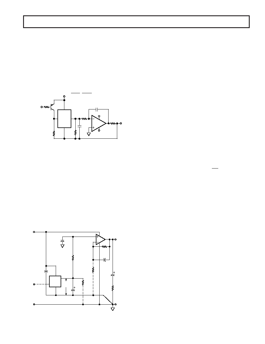
Figure 8. A Negative Precision Voltage Reference That
Uses No Precision Resistors Exhibits High Output Current
Drive
A High Output Current, Buffered Reference/Regulator
Many applications require stable voltage outputs relatively close
in potential to an unregulated input source. This “low dropout”
type of reference/regulator is readily implemented with a rail-to-
rail output op amp, and is particularly useful when using a
higher current device such as the OP179/OP279. A typical
example is the 3.3 V or 4.5 V reference voltage developed from
a 5 V system source. Generating these voltages requires a three-
terminal reference, such as the REF196 (3.3 V) or the REF194
(4.5 V), both of which feature low power, with sourcing outputs
of 30 mA or less. Figure 9 shows how such a reference can be
outfitted with an OP179/OP279 buffer for higher currents and/
or voltage levels, plus sink and source load capability.
C2
0.1 F
R2
10k
1%
U2
1/2 OP279
VOUT1 =
3.3V @ 30mA
R5
1
C5
10 F/25V
TANTALUM
R1
10k
1%
C1
0.1 F
VS
5V
VOUT2=
3.3V
C4
1 F
6
2
3
4
VOUT
COMMON
C3
0.1 F
VC
ON/OFF
CONTROL
INPUT CMOS HI
(OR OPEN) = ON
LO = OFF
VS
COMMON
R3
(SEE TEXT)
R4
3.3k
U1
REF196
Figure 9. A High Output Current Reference/Regulator
The low dropout performance of this circuit is provided by stage
U2, one-half of an OP179/OP279 connected as a follower/buffer
for the basic reference voltage produced by U1. The low voltage
saturation characteristic of the OP179/OP279 allows up to 30 mA
of load current in the illustrated use, as a 5 V to 3.3 V converter
with high dc accuracy. In fact, the dc output voltage change for
a 30 mA load current delta measures less than 1 mV. This
corresponds to an equivalent output impedance of < 0.03
. In
this application, the stable 3.3 V from U1 is applied to U2
through a noise filter, R1-C1. U2 replicates the U1 voltage
within a few mV, but at a higher current output at VOUT1, with
the ability to both sink and source output current(s)—unlike
most IC references. R2 and C2 in the feedback path of U2
provide bias compensation for lowest dc error and additional
noise filtering.
Transient performance of the reference/regulator for a 10 mA
step change in load current is also quite good and is determined
largely by the R5-C5 output network. With values as shown, the
transient is about 10 mV peak and settles to within 2 mV in 8
s,
for either polarity. Although room exists for optimizing the
transient response, any changes to the R5-C5 network should
be verified by experiment to preclude the possibility of excessive
ringing with some capacitor types.
To scale VOUT2 to another (higher) output level, the optional
resistor R3 (shown dotted) is added, causing the new VOUT1 to
become:
VV
R
OUT1
OUT2
=× +
1
2
3
As an example, for a VOUT1 = 4.5 V, and VOUT2 = 2.5 V from a
REF192, the gain required of U2 is 1.8 times, so R2 and R3
would be chosen for a ratio of 0.8:1, or 18 k
:22.5 k. Note that
for the lowest VOUT1 dc error, the parallel combination of R2 and
R3 should be maintained equal to R1 (as here), and the R2-R3
resistors should be stable, close tolerance metal film types.
The circuit can be used as shown as either a 5 V to 3.3 V reference/
regulator, or it can be used with ON/OFF control. By driving
Pin 3 of U1 with a logic control signal as noted, the output is
switched ON/OFF. Note that when ON/OFF control is used,
resistor R4 should be used with U1 to speed ON-OFF switching.
Direct Access Arrangement for Telephone Line Interface
Figure 10 illustrates a 5 V only transmit/receive telephone line
interface for 110
transmission systems. It allows full duplex
transmission of signals on a transformer coupled 110
line in
a differential manner. Amplifier A1 provides gain that can be
adjusted to meet the modem output drive requirements. Both
A1 and A2 are configured to apply the largest possible signal on a
single supply to the transformer. Because of the OP179/OP279’s
high output current drive and low dropout voltage, the largest
signal available on a single 5 V supply is approximately 4.5 V p-p
into a 110
transmission system. Amplifier A3 is configured as
a difference amplifier to extract the receive signal from the
transmission line for amplification by A4. A4’s gain can be adjusted
in the same manner as A1’s to meet the modem’s input signal
requirements. Standard resistor values permit the use of SIP
(Single In-line Package) format resistor arrays. Couple this with
the OP179/OP279’s 8-lead SOIC footprint and this circuit
offers a compact, cost-sensitive solution.
相关PDF资料 |
PDF描述 |
|---|---|
| P6KE56ARL | TVS ZENER UNIDIR 600W 56V AXIAL |
| MMK25-026 | CONN RACK/PANEL 26POS 5A |
| P6KE51ARL | TVS ZENER UNIDIR 600W 51V AXIAL |
| AD8031ARZ-REEL | IC OPAMP VF R-R LP LDIST 8SOIC |
| MMA23-018 | CONN RACK/PANEL 18POS 5A |
相关代理商/技术参数 |
参数描述 |
|---|---|
| OP279GSZ-REEL7 | 功能描述:IC OPAMP GP R-R 5MHZ DUAL 8SOIC RoHS:是 类别:集成电路 (IC) >> Linear - Amplifiers - Instrumentation 系列:- 标准包装:1,000 系列:- 放大器类型:电压反馈 电路数:4 输出类型:满摆幅 转换速率:33 V/µs 增益带宽积:20MHz -3db带宽:30MHz 电流 - 输入偏压:2nA 电压 - 输入偏移:3000µV 电流 - 电源:2.5mA 电流 - 输出 / 通道:30mA 电压 - 电源,单路/双路(±):4.5 V ~ 16.5 V,±2.25 V ~ 8.25 V 工作温度:-40°C ~ 85°C 安装类型:表面贴装 封装/外壳:14-SOIC(0.154",3.90mm 宽) 供应商设备封装:14-SOIC 包装:带卷 (TR) |
| OP27A | 制造商:TI 制造商全称:Texas Instruments 功能描述:LOW-NOISE HIGH-SPEED PRECISION OPERATIONAL AMPLIFIERS |
| OP-27A | 制造商:LINER 制造商全称:Linear Technology 功能描述:Low Noise, High Speed Precision Operational Amplifiers |
| OP27AFK | 制造商:TI 制造商全称:Texas Instruments 功能描述:LOW-NOISE HIGH-SPEED PRECISION OPERATIONAL AMPLIFIERS |
| OP27AFKB | 制造商:Texas Instruments 功能描述:OP Amp Single GP 制造商:Rochester Electronics LLC 功能描述:LOW NOISE PRECISION OP AMP - Bulk 制造商:Texas Instruments 功能描述:OP AMP SGL GP 22V 20LCCC - Rail/Tube |
发布紧急采购,3分钟左右您将得到回复。