参数资料
| 型号: | OP27GS-REEL7 |
| 厂商: | Analog Devices Inc |
| 文件页数: | 6/20页 |
| 文件大小: | 0K |
| 描述: | IC OPAMP GP 8MHZ LN PREC 8SOIC |
| 标准包装: | 1,000 |
| 放大器类型: | 通用 |
| 电路数: | 1 |
| 转换速率: | 2.8 V/µs |
| 增益带宽积: | 8MHz |
| 电流 - 输入偏压: | 15nA |
| 电压 - 输入偏移: | 30µV |
| 电压 - 电源,单路/双路(±): | ±4 V ~ 18 V |
| 工作温度: | -40°C ~ 85°C |
| 安装类型: | 表面贴装 |
| 封装/外壳: | 8-SOIC(0.154",3.90mm 宽) |
| 供应商设备封装: | 8-SO |
| 包装: | 带卷 (TR) |
| 其它名称: | OP27GS-REEL7-ND OP27GS-REEL7TR |
OP27
Rev. F | Page 14 of 20
APPLICATION INFORMATION
OP27 series units can be inserted directly into OP07 sockets
with or without removal of external compensation or nulling
components. Additionally, the OP27 can be fitted to unnulled
circuitry is in use, it should be modified or removed to ensure
correct OP27 operation. OP27 offset voltage can be nulled to
0 (or another desired setting) using a potentiometer (see
The OP27 provides stable operation with load capacitances of
up to 2000 pF and ±10 V swings; larger capacitances should be
decoupled with a 50 Ω resistor inside the feedback loop. The
OP27 is unity-gain stable.
Thermoelectric voltages generated by dissimilar metals at the
input terminal contacts can degrade the drift performance.
Best operation is obtained when both input contacts are
maintained at the same temperature.
+
–-
OP27
V–
V+
OUTPUT
RP
10k
Ω
1
7
6
4
8
3
2
00317-035
Figure 35. Offset Nulling Circuit
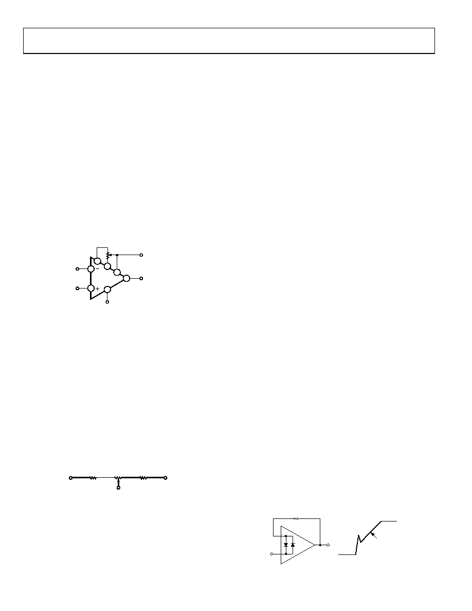
OFFSET VOLTAGE ADJUSTMENT
The input offset voltage of the OP27 is trimmed at wafer level.
However, if further adjustment of VOS is necessary, a 10 kΩ trim
Other potentiometer values from 1 kΩ to 1 MΩ can be used
with a slight degradation (0.1 μV/°C to 0.2 μV/°C) of TCVOS.
Trimming to a value other than zero creates a drift of approxi-
mately (VOS/300) μV/°C. For example, the change in TCVOS is
0.33 μV/°C if VOS is adjusted to 100 μV. The offset voltage
adjustment range with a 10 kΩ potentiometer is ±4 mV. If smaller
adjustment range is required, the nulling sensitivity can be
reduced by using a smaller potentiometer in conjunction with
fixed resistors. For example, Figure 36 shows a network that has
a 280 μV adjustment range.
1
8
4.7k
Ω
4.7k
Ω
1k
Ω POTT
V+
00317-036
Figure 36. Offset Voltage Adjustment
NOISE MEASUREMENTS
To measure the 80 nV p-p noise specification of the OP27 in
the 0.1 Hz to 10 Hz range, the following precautions must be
observed:
The device must be warmed up for at least five minutes.
As shown in the warm-up drift curve, the offset voltage
typically changes 4 μV due to increasing chip temperature
after power-up. In the 10-second measurement interval,
these temperature-induced effects can exceed tens-of-
nanovolts.
For similar reasons, the device has to be well-shielded
from air currents. Shielding minimizes thermocouple effects.
Sudden motion in the vicinity of the device can also
feedthrough to increase the observed noise.
The test time to measure 0.1 Hz to 10 Hz noise should not
exceed 10 seconds. As shown in the noise-tester frequency
response curve, the 0.1 Hz corner is defined by only one
zero. The test time of 10 seconds acts as an additional zero
to eliminate noise contributions from the frequency band
below 0.1 Hz.
A noise voltage density test is recommended when
measuring noise on a large number of units. A 10 Hz noise
voltage density measurement correlates well with a 0.1 Hz to
10 Hz p-p noise reading, since both results are determined
by the white noise and the location of the 1/f corner
frequency.
UNITY-GAIN BUFFER APPLICATIONS
When Rf ≤ 100 Ω and the input is driven with a fast, large
signal pulse (>1 V), the output waveform looks as shown in the
pulsed operation diagram (see Figure 37).
During the fast feedthrough-like portion of the output, the
input protection diodes effectively short the output to the input,
and a current, limited only by the output short-circuit protect-
ion, is drawn by the signal generator. With Rf ≥ 500 Ω, the
output is capable of handling the current requirements (IL ≤ 20 mA
at 10 V); the amplifier stays in its active mode and a smooth
transition occurs.
When Rf > 2 kΩ, a pole is created with Rf and the amplifier’s
input capacitance (8 pF) that creates additional phase shift and
reduces phase margin. A small capacitor (20 pF to 50 pF) in
parallel with Rf eliminates this problem.
+
–
OP27
Rf
2.8V/
μs
00317-
037
Figure 37. Pulsed Operation
相关PDF资料 |
PDF描述 |
|---|---|
| 1PMT26AT1G | TVS 200W 26V POWERMITE |
| MMB21-0341JU | CONN RACK/PANEL 34POS 5A |
| AD8656WARMZ-REEL | IC OPAMP GP R-R CMOS 28MHZ 8MSOP |
| MMB25-0201K1 | CONN RACK/PANEL 20POS 5A |
| 1PMT22AT1G | TVS 200W 22V POWERMITE |
相关代理商/技术参数 |
参数描述 |
|---|---|
| OP27GS-T | 功能描述:运算放大器 - 运放 RoHS:否 制造商:STMicroelectronics 通道数量:4 共模抑制比(最小值):63 dB 输入补偿电压:1 mV 输入偏流(最大值):10 pA 工作电源电压:2.7 V to 5.5 V 安装风格:SMD/SMT 封装 / 箱体:QFN-16 转换速度:0.89 V/us 关闭:No 输出电流:55 mA 最大工作温度:+ 125 C 封装:Reel |
| OP27GSZ | 功能描述:IC OPAMP GP 8MHZ LN PREC 8SOIC RoHS:是 类别:集成电路 (IC) >> Linear - Amplifiers - Instrumentation 系列:- 产品培训模块:Differential Circuit Design Techniques for Communication Applications 标准包装:1 系列:- 放大器类型:RF/IF 差分 电路数:1 输出类型:差分 转换速率:9800 V/µs 增益带宽积:- -3db带宽:2.9GHz 电流 - 输入偏压:3µA 电压 - 输入偏移:- 电流 - 电源:40mA 电流 - 输出 / 通道:- 电压 - 电源,单路/双路(±):3 V ~ 3.6 V 工作温度:-40°C ~ 85°C 安装类型:表面贴装 封装/外壳:16-VQFN 裸露焊盘,CSP 供应商设备封装:16-LFCSP-VQ 包装:剪切带 (CT) 产品目录页面:551 (CN2011-ZH PDF) 其它名称:ADL5561ACPZ-R7CT |
| OP27GSZ1 | 制造商:AD 制造商全称:Analog Devices 功能描述:Low Noise, Precision Operational Amplifier |
| OP27GSZ-REEL | 功能描述:IC OPAMP GP 8MHZ LN PREC 8SOIC RoHS:是 类别:集成电路 (IC) >> Linear - Amplifiers - Instrumentation 系列:- 标准包装:2,500 系列:- 放大器类型:通用 电路数:1 输出类型:满摆幅 转换速率:0.11 V/µs 增益带宽积:350kHz -3db带宽:- 电流 - 输入偏压:4nA 电压 - 输入偏移:20µV 电流 - 电源:260µA 电流 - 输出 / 通道:20mA 电压 - 电源,单路/双路(±):2.7 V ~ 36 V,±1.35 V ~ 18 V 工作温度:-40°C ~ 85°C 安装类型:表面贴装 封装/外壳:8-SOIC(0.154",3.90mm 宽) 供应商设备封装:8-SO 包装:带卷 (TR) |
| OP27GSZ-REEL1 | 制造商:AD 制造商全称:Analog Devices 功能描述:Low Noise, Precision Operational Amplifier |
发布紧急采购,3分钟左右您将得到回复。