参数资料
| 型号: | OP27GS-REEL7 |
| 厂商: | Analog Devices Inc |
| 文件页数: | 9/20页 |
| 文件大小: | 0K |
| 描述: | IC OPAMP GP 8MHZ LN PREC 8SOIC |
| 标准包装: | 1,000 |
| 放大器类型: | 通用 |
| 电路数: | 1 |
| 转换速率: | 2.8 V/µs |
| 增益带宽积: | 8MHz |
| 电流 - 输入偏压: | 15nA |
| 电压 - 输入偏移: | 30µV |
| 电压 - 电源,单路/双路(±): | ±4 V ~ 18 V |
| 工作温度: | -40°C ~ 85°C |
| 安装类型: | 表面贴装 |
| 封装/外壳: | 8-SOIC(0.154",3.90mm 宽) |
| 供应商设备封装: | 8-SO |
| 包装: | 带卷 (TR) |
| 其它名称: | OP27GS-REEL7-ND OP27GS-REEL7TR |
OP27
Rev. F | Page 17 of 20
CA
RA
R1
33k
R2
5k
TAPE
HEAD
0.47F
0.01F
10
15k
T1 = 3180s
T2 = 50s
OP27
+
–
00
31
7-
0
42
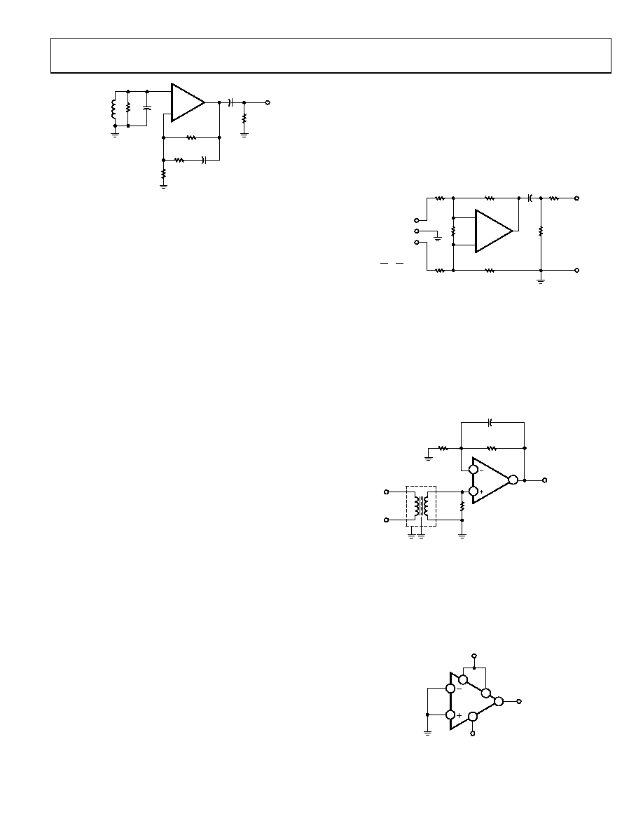
Figure 42. Tape Head Preamplifier
While the tape equalization requirement has a flat high
frequency gain above 3 kHz (T2 = 50 μs), the amplifier need
not be stabilized for unity gain. The decompensated OP37
provides a greater bandwidth and slew rate. For many applica-
tions, the idealized time constants shown can require trimming
of R1 and R2 to optimize frequency response for nonideal tape
head performance and other factors (see the References
section).
The network values of the configuration yield a 50 dB gain at
1 kHz, and the dc gain is greater than 70 dB. Thus, the worst-
case output offset is just over 500 mV. A single 0.47 μF output
capacitor can block this level without affecting the dynamic
range.
The tape head can be coupled directly to the amplifier input,
because the worst-case bias current of 80 nA with a 400 mH,
100 μ inch head (such as the PRB2H7K) is not troublesome.
Amplifier bias-current transients that can magnetize a head
present one potential tape head problem. The OP27 and OP37
are free of bias current transients upon power-up or power-
down. It is always advantageous to control the speed of power
supply rise and fall to eliminate transients.
In addition, the dc resistance of the head should be carefully
controlled and preferably below 1 kΩ. For this configuration,
the bias current induced offset voltage can be greater than the
100 pV maximum offset if the head resistance is not sufficiently
controlled.
A simple, but effective, fixed gain transformerless microphone
preamp (Figure 43) amplifies differential signals from low
impedance microphones by 50 dB and has an input impedance
of 2 kΩ. Because of the high working gain of the circuit, an
OP37 helps to preserve bandwidth, which is 110 kHz. As the
OP37 is a decompensated device (minimum stable gain of 5), a
dummy resistor, Rp, may be necessary if the microphone is to be
unplugged. Otherwise, the 100% feedback from the open input
can cause the amplifier to oscillate.
Common-mode input noise rejection will depend upon the
match of the bridge-resistor ratios. Either close tolerance (0.1%)
types should be used, or R4 should be trimmed for best CMRR.
All resistors should be metal film types for best stability and low
noise.
Noise performance of this circuit is limited more by the Input
Resistors R1 and R2 than by the op amp, as R1 and R2 each
generate a 4 nV/√Hz noise, while the op amp generates a
3.2 nV/√Hz noise. The rms sum of these predominant noise
sources is about 6 nV/√Hz, equivalent to 0.9 μV in a 20 kHz
noise bandwidth, or nearly 61 dB below a 1 mV input signal.
Measurements confirm this predicted performance.
LOW IMPEDANCE
MICROPHONE INPUT
(Z = 50 TO 200)
C1
5mF
R1
1k
R3
316k
R6
100
R4
316k
R2
1k
RP
30k
OUTPUT
R3
R1
R4
R2
=
OP27/
OP37
+
–
R7
10k
00
31
7-
0
43
Figure 43. Fixed Gain Transformerless Microphone Preamplifier
For applications demanding appreciably lower noise, a high
quality microphone transformer coupled preamplifier (Figure
44) incorporates the internally compensated OP27. T1 is a JE-
115K-E 150 Ω/15 kΩ transformer that provides an optimum
source resistance for the OP27 device. The circuit has an overall
gain of 40 dB, the product of the transformer’s voltage setup and
the op amp’s voltage gain.
JENSEN TRANSFORMERS
A1
OP27
R3
100
R1
121
R2
1100
C2
1800pF
OUTPUT
150
SOURCE
T11
T1 – JENSEN JE – 115K – E
1
3
6
2
00
31
7-
0
44
Figure 44. High Quality Microphone Transformer Coupled Preamplifier
Gain can be trimmed to other levels, if desired, by adjusting R2
or R1. Because of the low offset voltage of the OP27, the output
offset of this circuit is very low, 1.7 mV or less, for a 40 dB gain.
The typical output blocking capacitor can be eliminated in such
cases, but it is desirable for higher gains to eliminate switching
transients.
OP27
–18V
+18V
8
7
6
4
3
2
00317-045
Figure 45. Burn-In Circuit
相关PDF资料 |
PDF描述 |
|---|---|
| 1PMT26AT1G | TVS 200W 26V POWERMITE |
| MMB21-0341JU | CONN RACK/PANEL 34POS 5A |
| AD8656WARMZ-REEL | IC OPAMP GP R-R CMOS 28MHZ 8MSOP |
| MMB25-0201K1 | CONN RACK/PANEL 20POS 5A |
| 1PMT22AT1G | TVS 200W 22V POWERMITE |
相关代理商/技术参数 |
参数描述 |
|---|---|
| OP27GS-T | 功能描述:运算放大器 - 运放 RoHS:否 制造商:STMicroelectronics 通道数量:4 共模抑制比(最小值):63 dB 输入补偿电压:1 mV 输入偏流(最大值):10 pA 工作电源电压:2.7 V to 5.5 V 安装风格:SMD/SMT 封装 / 箱体:QFN-16 转换速度:0.89 V/us 关闭:No 输出电流:55 mA 最大工作温度:+ 125 C 封装:Reel |
| OP27GSZ | 功能描述:IC OPAMP GP 8MHZ LN PREC 8SOIC RoHS:是 类别:集成电路 (IC) >> Linear - Amplifiers - Instrumentation 系列:- 产品培训模块:Differential Circuit Design Techniques for Communication Applications 标准包装:1 系列:- 放大器类型:RF/IF 差分 电路数:1 输出类型:差分 转换速率:9800 V/µs 增益带宽积:- -3db带宽:2.9GHz 电流 - 输入偏压:3µA 电压 - 输入偏移:- 电流 - 电源:40mA 电流 - 输出 / 通道:- 电压 - 电源,单路/双路(±):3 V ~ 3.6 V 工作温度:-40°C ~ 85°C 安装类型:表面贴装 封装/外壳:16-VQFN 裸露焊盘,CSP 供应商设备封装:16-LFCSP-VQ 包装:剪切带 (CT) 产品目录页面:551 (CN2011-ZH PDF) 其它名称:ADL5561ACPZ-R7CT |
| OP27GSZ1 | 制造商:AD 制造商全称:Analog Devices 功能描述:Low Noise, Precision Operational Amplifier |
| OP27GSZ-REEL | 功能描述:IC OPAMP GP 8MHZ LN PREC 8SOIC RoHS:是 类别:集成电路 (IC) >> Linear - Amplifiers - Instrumentation 系列:- 标准包装:2,500 系列:- 放大器类型:通用 电路数:1 输出类型:满摆幅 转换速率:0.11 V/µs 增益带宽积:350kHz -3db带宽:- 电流 - 输入偏压:4nA 电压 - 输入偏移:20µV 电流 - 电源:260µA 电流 - 输出 / 通道:20mA 电压 - 电源,单路/双路(±):2.7 V ~ 36 V,±1.35 V ~ 18 V 工作温度:-40°C ~ 85°C 安装类型:表面贴装 封装/外壳:8-SOIC(0.154",3.90mm 宽) 供应商设备封装:8-SO 包装:带卷 (TR) |
| OP27GSZ-REEL1 | 制造商:AD 制造商全称:Analog Devices 功能描述:Low Noise, Precision Operational Amplifier |
发布紧急采购,3分钟左右您将得到回复。