参数资料
| 型号: | OP293FSZ-REEL7 |
| 厂商: | Analog Devices Inc |
| 文件页数: | 2/16页 |
| 文件大小: | 0K |
| 描述: | IC OPAMP GP 35KHZ DUAL 8SOIC |
| 设计资源: | 4 mA-to-20 mA Loop-Powered Temperature Monitor Using ADuC7060/1 (CN0145) |
| 标准包装: | 1 |
| 放大器类型: | 通用 |
| 电路数: | 2 |
| 输出类型: | 满摆幅 |
| 转换速率: | 0.015 V/µs |
| 增益带宽积: | 35kHz |
| 电流 - 输入偏压: | 20nA |
| 电压 - 输入偏移: | 250µV |
| 电流 - 电源: | 30µA |
| 电流 - 输出 / 通道: | 25mA |
| 电压 - 电源,单路/双路(±): | 1.7 V ~ 36 V,±0.85 V ~ 18 V |
| 工作温度: | -40°C ~ 125°C |
| 安装类型: | 表面贴装 |
| 封装/外壳: | 8-SOIC(0.154",3.90mm 宽) |
| 供应商设备封装: | 8-SOIC |
| 包装: | 标准包装 |
| 产品目录页面: | 768 (CN2011-ZH PDF) |
| 其它名称: | OP293FSZ-REEL7DKR |
REV. B
OP193/OP293/OP493
–10–
Driving Capacitive Loads
OP193 family amplifiers are unconditionally stable with capacitive
loads less than 200 pF. However, the small signal, unity-gain
overshoot will improve if a resistive load is added. For example,
transient overshoot is 20% when driving a 1000 pF/ 10 k
load.
When driving large capacitive loads in unity-gain configurations,
an in-the-loop compensation technique is recommended as
illustrated in Figure 6.
Input Overvoltage Protection
As previously mentioned, the OP193 family of op amps use a
PNP input stage with protection resistors in series with the
inverting and noninverting inputs. The high breakdown of the
PNP transistors, coupled with the protection resistors, provides
a large amount of input protection from over voltage conditions.
The inputs can therefore be taken 20 V beyond either supply
without damaging the amplifier.
Output Phase Reversal—OP193
The OP193’s input PNP collector-base junction can be forward-
biased if the inputs are brought more than one diode drop (0.7 V)
below ground. When this happens to the noninverting input, Q4
of the cascode stage turns on and the output goes high. If the
positive input signal can go below ground, phase reversal can be
prevented by clamping the input to the negative supply (i.e.,
GND) with a diode. The reverse leakage of the diode will, of
course, add to the input bias current of the amplifier. If input bias
current is not critical, a 1N914 will add less than 10 nA of leak-
age. However, its leakage current will double for every 10
°C
increase in ambient temperature. For critical applications, the
collector-base junction of a 2N3906 transistor will add only about
10 pA of additional bias current. To limit the current through the
diode under fault conditions, a 1 k
resistor is recommended in
series with the input. (The OP193’s internal current limiting
resistors will not protect the external diode.)
Output Phase Reversal—OP293 and OP493
The OP293 and OP493 include lateral PNP transistors Q7 and
Q8 to protect against phase reversal. If an input is brought more
than one diode drop (
≈0.7 V) below ground, Q7 and Q8 com-
bine to level shift the entire cascode stage, including the bias to
Q3 and Q4, simultaneously. In this case Q4 will not saturate
and the output remains low.
The OP293 and OP493 do not exhibit output phase reversal for
inputs up to –5 V below V– at +25
°C. The phase reversal limit
at +125
°C is about –3 V. If the inputs can be driven below these
levels, an external clamp diode, as discussed in the previous
section, should be added.
Battery-Powered Applications
OP193 series op amps can be operated on a minimum supply
voltage of 1.7 V, and draw only 13
A of supply current per
amplifier from a 2.0 V supply. In many battery-powered circuits,
OP193 devices can be continuously operated for thousands of
hours before requiring battery replacement, thus reducing
equipment downtime and operating cost.
High performance portable equipment and instruments fre-
quently use lithium cells because of their long shelf life, light
weight, and high energy density relative to older primary cells.
Most lithium cells have a nominal output voltage of 3 V and are
noted for a flat discharge characteristic. The low supply voltage
requirement of the OP193, combined with the flat discharge
characteristic of the lithium cell, indicates that the OP193 can
be operated over the entire useful life of the cell. Figure 3 shows
the typical discharge characteristic of a 1 AH lithium cell power-
ing the OP193, OP293, and OP493, with each amplifier, in
turn, driving 2.1 Volts into a 100 k
load.
LITHIUM
SULPHUR
DIOXIDE
CELL
VOLTAGE
–
V
5000
0
2
1
HOURS
3
1000
7000
2000
3000
4000
6000
4
0
OP493
OP293
OP193
Figure 3. Lithium Sulfur Dioxide Cell Discharge Character-
istic with OP193 Family and 100 k
Loads
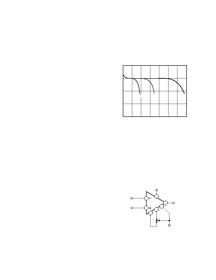
Input Offset Voltage Nulling
The OP193 provides two offset nulling terminals that can be
used to adjust the OP193’s internal VOS. In general, operational
amplifier terminals should never be used to adjust system offset
voltages. The offset null circuit of Figure 4 provides about
±7 mV of offset adjustment range. A 100 k resistor placed in
series with the wiper arm of the offset null potentiometer, as
shown in Figure 5, reduces the offset adjustment range to 400
V
and is recommended for applications requiring high null resolu-
tion. Offset nulling does not adversely affect TCVOS performance,
providing that the trimming potentiometer temperature coeffi-
cient does not exceed
±100 ppm/°C.
6
5
7
4
1
2
3
V–
V+
OP193
100k
Figure 4. Offset Nulling Circuit
相关PDF资料 |
PDF描述 |
|---|---|
| KDE1235PFB3-8 MS | FAN 12VDC 35X10MM .7W 3.8CFM |
| 68046-335LF | CONN RCPT 70POS .100" DBL SMD |
| SFML-150-02-S-D | CONN RECPT 100POS 1.27MM GLD SMD |
| PBC10SFBN | CONN HEADER .100 SINGL STR 10POS |
| MMS-140-01-L-SH | CONN RCPT 2MM 40POS SGL HORZ PCB |
相关代理商/技术参数 |
参数描述 |
|---|---|
| OP293FSZ-REEL71 | 制造商:AD 制造商全称:Analog Devices 功能描述:Precision, Micropower Operational Amplifiers |
| OP293FSZ-REEL7-DASSAULT | 制造商:Analog Devices 功能描述: |
| OP293GBC | 制造商:AD 制造商全称:Analog Devices 功能描述:Precision, Micropower Operational Amplifiers |
| OP294 | 功能描述:红外发射源 Infrared 890nm RoHS:否 制造商:Fairchild Semiconductor 波长:880 nm 射束角:+/- 25 辐射强度: 最大工作温度:+ 100 C 最小工作温度:- 40 C 封装 / 箱体:Side Looker 封装:Bulk |
| OP295 | 制造商:AD 制造商全称:Analog Devices 功能描述:DUAL/QUAD RAIL-TO-RAIL OPERATIONAL AMPLIFIERS |
发布紧急采购,3分钟左右您将得到回复。