参数资料
| 型号: | OP295GPZ |
| 厂商: | Analog Devices Inc |
| 文件页数: | 16/16页 |
| 文件大小: | 0K |
| 描述: | IC OPAMP GP R-R 85KHZ DUAL 8DIP |
| 标准包装: | 50 |
| 放大器类型: | 通用 |
| 电路数: | 2 |
| 输出类型: | 满摆幅 |
| 转换速率: | 0.03 V/µs |
| 增益带宽积: | 85kHz |
| 电流 - 输入偏压: | 7nA |
| 电压 - 输入偏移: | 300µV |
| 电流 - 电源: | 175µA |
| 电流 - 输出 / 通道: | 25mA |
| 电压 - 电源,单路/双路(±): | 3 V ~ 36 V,±1.5 V ~ 18 V |
| 工作温度: | -40°C ~ 125°C |
| 安装类型: | 通孔 |
| 封装/外壳: | 8-DIP(0.300",7.62mm) |
| 供应商设备封装: | 8-PDIP |
| 包装: | 管件 |
| 产品目录页面: | 768 (CN2011-ZH PDF) |
OP295/OP495
Rev. G | Page 9 of 16
APPLICATIONS
RAIL-TO-RAIL APPLICATION INFORMATION
The OP295/OP495 have a wide common-mode input range
extending from ground to within about 800 mV of the positive
supply. There is a tendency to use the OP295/OP495 in buffer
applications where the input voltage could exceed the common-
mode input range. This can initially appear to work because of
the high input range and rail-to-rail output range. But above the
common-mode input range, the amplifier is, of course, highly
nonlinear. For this reason, there must be some minimal amount
of gain when rail-to-rail output swing is desired. Based on the
input common-mode range, this gain should be at least 1.2.
LOW DROP-OUT REFERENCE
The OP295/OP495 can be used to gain up a 2.5 V or other low
voltage reference to 4.5 V for use with high resolution ADCs
that operate from 5 V only supplies. The circuit in Figure 19
supplies up to 10 mA. Its no-load drop-out voltage is only
20 mV. This circuit supplies over 3.5 mA with a 5 V supply.
4
2
6
–
+
1/2
OP295/OP495
VOUT =4.5V
5V
16k
10
20k
0.001F
REF43
1F TO
10F
00
33
1-
01
7
Figure 19. 4.5 V, Low Drop-Out Reference
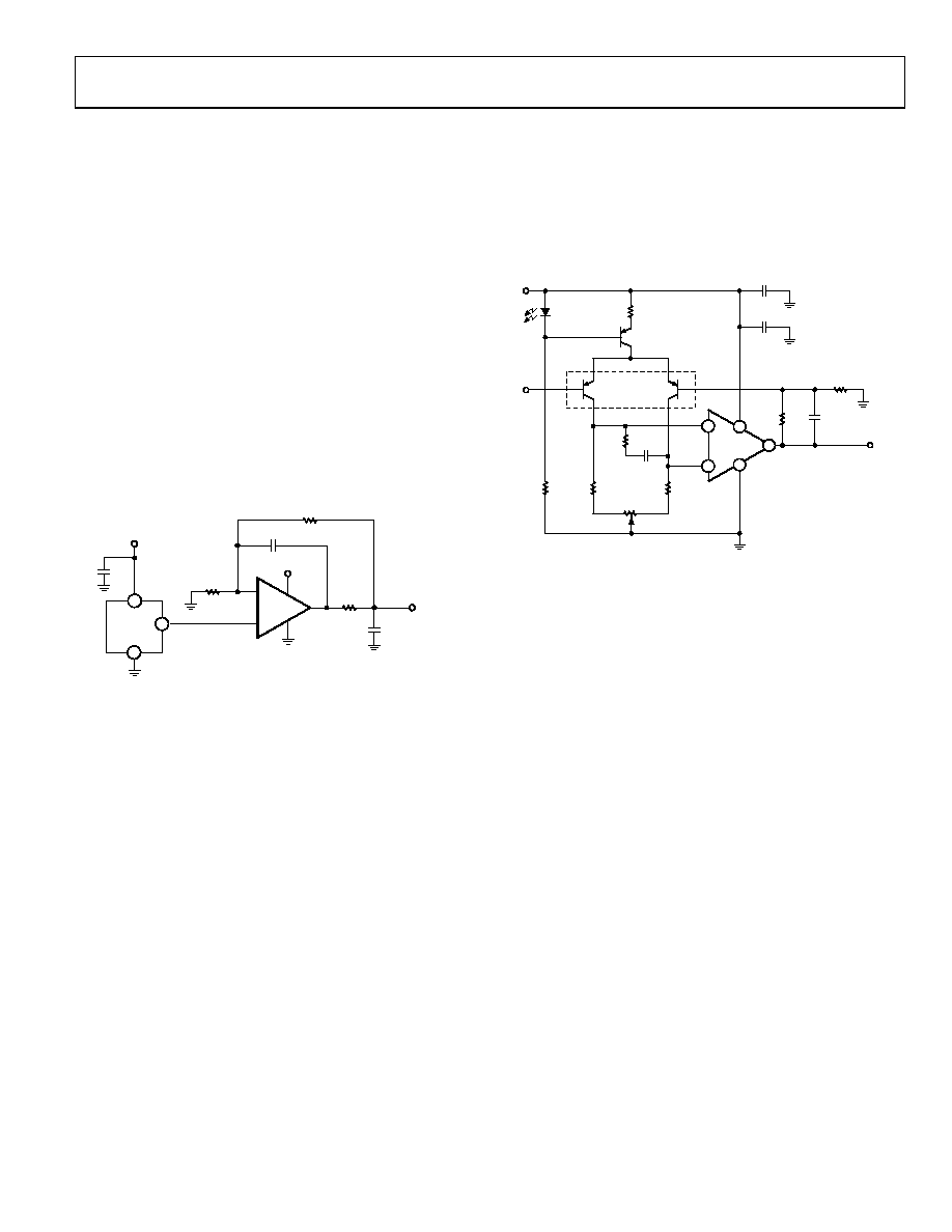
LOW NOISE, SINGLE-SUPPLY PREAMPLIFIER
Most single-supply op amps are designed to draw low supply
current at the expense of having higher voltage noise. This tradeoff
may be necessary because the system must be powered by a
battery. However, this condition is worsened because all circuit
resistances tend to be higher; as a result, in addition to the op
amp’s voltage noise, Johnson noise (resistor thermal noise) is
also a significant contributor to the total noise of the system.
The choice of monolithic op amps that combine the character-
istics of low noise and single-supply operation is rather limited.
Most single-supply op amps have noise on the order of 30 nV/√Hz
to 60 nV/√Hz, and single-supply amplifiers with noise below
5 nV/√Hz do not exist.
To achieve both low noise and low supply voltage operation,
discrete designs may provide the best solution. The circuit in
Figure 20 uses the OP295/OP495 rail-to-rail amplifier and a
matched PNP transistor pair—the MAT03—to achieve zero-
in/zero-out single-supply operation with an input voltage noise
of 3.1 nV/√Hz at 100 Hz.
R5 and R6 set the gain of 1000, making this circuit ideal for
maximizing dynamic range when amplifying low level signals in
single-supply applications. The OP295/OP495 provide rail-to-
rail output swings, allowing this circuit to operate with 0 V to
5 V outputs. Only half of the OP295/OP495 is used, leaving the
other uncommitted op amp for use elsewhere.
1
2
3
4
8
–
+
+–
26
5
3
7
1
Q1
Q2
MAT03
0.1F
R1
LED
R4
R3
OP295/OP495
10F
R6
10
VOUT
C2
10F
R5
10k
Q2
2N3906
R7
510
R2
27k
R8
100
C1
1500pF
VIN
003
31-
01
8
Figure 20. Low Noise Single-Supply Preamplifier
The input noise is controlled by the MAT03 transistor pair
and the collector current level. Increasing the collector current
reduces the voltage noise. This particular circuit was tested
with 1.85 mA and 0.5 mA of current. Under these two cases,
the input voltage noise was 3.1 nV/√Hz and 10 nV/√Hz, respect-
ively. The high collector currents do lead to a tradeoff in supply
current, bias current, and current noise. All of these parameters
increase with increasing collector current. For example, typically
the MAT03 has an hFE = 165. This leads to bias currents of 11 μA
and 3 μA, respectively.
Based on the high bias currents, this circuit is best suited for
applications with low source impedance such as magnetic
pickups or low impedance strain gauges. Furthermore, a high
source impedance degrades the noise performance. For
example, a 1 kΩ resistor generates 4 nV/√Hz of broadband
noise, which is already greater than the noise of the preamp.
The collector current is set by R1 in combination with the LED
and Q2. The LED is a 1.6 V Zener diode that has a temperature
coefficient close to that of the Q2 base-emitter junction, which
provides a constant 1.0 V drop across R1. With R1 equal to
270 Ω, the tail current is 3.7 mA and the collector current is half
that, or 1.85 mA. The value of R1 can be altered to adjust the
collector current. When R1 is changed, R3 and R4 should also
be adjusted. To maintain a common-mode input range that
includes ground, the collectors of the Q1 and Q2 should not go
above 0.5 V; otherwise, they could saturate. Thus, R3 and R4
must be small enough to prevent this condition. Their values
and the overall performance for two different values of R1 are
summarized in Table 6.
相关PDF资料 |
PDF描述 |
|---|---|
| PBC22SFAN | CONN HEADER .100 SINGL STR 22POS |
| 1.5SMC39AT3G | TVS ZENER UNIDIR 1500W 39V SMC |
| AD711KRZ | IC OPAMP BIFET PREC 25MA 8SOIC |
| PBC11SADN | CONN HEADER .100 SINGL STR 11POS |
| OP213FPZ | IC OPAMP GP 3.4MHZ DUAL LN 8DIP |
相关代理商/技术参数 |
参数描述 |
|---|---|
| OP295GS | 功能描述:IC OPAMP GP R-R 85KHZ DUAL 8SOIC RoHS:否 类别:集成电路 (IC) >> Linear - Amplifiers - Instrumentation 系列:- 标准包装:50 系列:- 放大器类型:J-FET 电路数:2 输出类型:- 转换速率:13 V/µs 增益带宽积:3MHz -3db带宽:- 电流 - 输入偏压:65pA 电压 - 输入偏移:3000µV 电流 - 电源:1.4mA 电流 - 输出 / 通道:- 电压 - 电源,单路/双路(±):7 V ~ 36 V,±3.5 V ~ 18 V 工作温度:-40°C ~ 85°C 安装类型:通孔 封装/外壳:8-DIP(0.300",7.62mm) 供应商设备封装:8-PDIP 包装:管件 |
| OP295GS | 制造商:Analog Devices 功能描述:SEMICONDUCTORSLINEAR |
| OP295GSREEL | 制造商:ANALOG 功能描述:NEW |
| OP295GS-REEL | 功能描述:IC OPAMP GP R-R 85KHZ DUAL 8SOIC RoHS:否 类别:集成电路 (IC) >> Linear - Amplifiers - Instrumentation 系列:- 其它有关文件:Automotive Product Guide 产品培训模块:Lead (SnPb) Finish for COTS Obsolescence Mitigation Program 标准包装:1 系列:- 放大器类型:通用 电路数:1 输出类型:满摆幅 转换速率:3 V/µs 增益带宽积:10MHz -3db带宽:- 电流 - 输入偏压:1pA 电压 - 输入偏移:70µV 电流 - 电源:2.5mA 电流 - 输出 / 通道:48mA 电压 - 电源,单路/双路(±):2.7 V ~ 5.5 V,±1.35 V ~ 2.75 V 工作温度:-40°C ~ 125°C 安装类型:表面贴装 封装/外壳:SOT-23-6 供应商设备封装:SOT-6 包装:Digi-Reel® 其它名称:MAX4475AUT#TG16DKR |
| OP295GS-REEL7 | 功能描述:IC OPAMP GP R-R 85KHZ DUAL 8SOIC RoHS:否 类别:集成电路 (IC) >> Linear - Amplifiers - Instrumentation 系列:- 产品培训模块:Lead (SnPb) Finish for COTS Obsolescence Mitigation Program 标准包装:1 系列:- 放大器类型:电流检测 电路数:1 输出类型:- 转换速率:- 增益带宽积:125kHz -3db带宽:- 电流 - 输入偏压:- 电压 - 输入偏移:100µV 电流 - 电源:1.1µA 电流 - 输出 / 通道:- 电压 - 电源,单路/双路(±):- 工作温度:-40°C ~ 85°C 安装类型:表面贴装 封装/外壳:4-WFBGA,CSPBGA 供应商设备封装:4-UCSP(2x2) 包装:剪切带 (CT) 其它名称:MAX9634WERS+TCT |
发布紧急采购,3分钟左右您将得到回复。