参数资料
| 型号: | OP295GPZ |
| 厂商: | Analog Devices Inc |
| 文件页数: | 3/16页 |
| 文件大小: | 0K |
| 描述: | IC OPAMP GP R-R 85KHZ DUAL 8DIP |
| 标准包装: | 50 |
| 放大器类型: | 通用 |
| 电路数: | 2 |
| 输出类型: | 满摆幅 |
| 转换速率: | 0.03 V/µs |
| 增益带宽积: | 85kHz |
| 电流 - 输入偏压: | 7nA |
| 电压 - 输入偏移: | 300µV |
| 电流 - 电源: | 175µA |
| 电流 - 输出 / 通道: | 25mA |
| 电压 - 电源,单路/双路(±): | 3 V ~ 36 V,±1.5 V ~ 18 V |
| 工作温度: | -40°C ~ 125°C |
| 安装类型: | 通孔 |
| 封装/外壳: | 8-DIP(0.300",7.62mm) |
| 供应商设备封装: | 8-PDIP |
| 包装: | 管件 |
| 产品目录页面: | 768 (CN2011-ZH PDF) |
OP295/OP495
Rev. G | Page 11 of 16
V+
–
+
–
+
5
3
2
1
6
8
4
7
1/2
OP295/
OP495
1/2
OP295/
OP495
+
–
VIN
VO
R4
100k
R3
20k
R2
20k
R1
100k
VREF
RG
VO =
(5+ 200k) VIN+VREF
RG
00
33
1-
0
22
Figure 24. Single-Supply Instrumentation Amplifier
Resistor RG sets the gain of the instrumentation amplifier.
Minimum gain is 6 (with no RG). All resistors should be matched
in absolute value as well as temperature coefficient to maximize
common-mode rejection performance and minimize drift. This
instrumentation amplifier can operate from a supply voltage as
low as 3 V.
SINGLE-SUPPLY RTD THERMOMETER AMPLIFIER
This RTD amplifier takes advantage of the rail-to-rail swing of
the OP295/OP495 to achieve a high bridge voltage in spite of a
low 5 V supply. The OP295/OP495 amplifier servos a constant
200 μA current to the bridge. The return current drops across
the parallel resistors 6.19 kΩ and 2.55 MΩ, developing a voltage
that is servoed to 1.235 V, which is established by the AD589
band gap reference. The 3-wire RTD provides an equal line
resistance drop in both 100 Ω legs of the bridge, thus improving
the accuracy.
The AMP04 amplifies the differential bridge signal and converts
it to a single-ended output. The gain is set by the series resis-
tance of the 332 Ω resistor plus the 50 Ω potentiometer. The
gain scales the output to produce a 4.5 V full scale. The 0.22 μF
capacitor to the output provides a 7 Hz low-pass filter to keep
noise at a minimum.
ZERO ADJ
AD589
37.4k
5V
1.235
3
2
4
5
6
8
1
7
5V
AMP04
50
332
0.22F
VO
–
+
2
3
1
+
–
200
10-TURNS
26.7k
0.5%
26.7k
0.5%
100
RTD
100
0.5%
2.55M
1%
6.19k
1%
1/2
OP295/
OP495
4.5V = 450°C
0V = 0°C
0
03
31
-0
23
Figure 25. Low Power RTD Amplifier
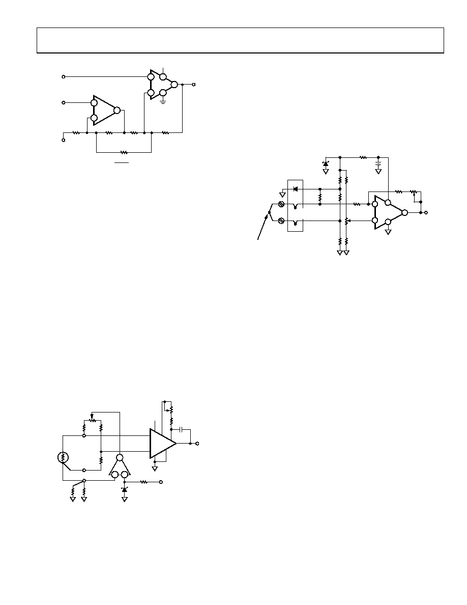
COLD JUNCTION COMPENSATED, BATTERY-
POWERED THERMOCOUPLE AMPLIFIER
The 150 μA quiescent current per amplifier consumption of the
OP295/OP495 makes them useful for battery-powered temperature
measuring instruments. The K-type thermocouple terminates
into an isothermal block where the terminated junctions’ ambient
temperatures can be continuously monitored and corrected by
summing an equal but opposite thermal EMF to the amplifier,
thereby canceling the error introduced by the cold junctions.
AD589
ALUMEL
CHROMEL
AL
CR
1N914
24.9k
1.235V
9V
1.33M
20k
2
3
4
8
–
+
–
+
–
+
1
COLD
JUNCTIONS
ISOTHERMAL
BLOCK
K-TYPE
THERMOCOUPLE
40.7V/°C
VO
5V = 500°C
0V = 0°C
OP295/
OP495
SCALE
ADJUST
7.15k
1%
1.5M
1%
24.9k
1%
475
1%
2.1k
1%
24.3k
1%
4.99k
1%
500
10-TURN
ZERO
ADJUST
00
33
1-
0
24
Figure 26. Battery-Powered, Cold-Junction Compensated
Thermocouple Amplifier
To calibrate, immerse the thermocouple measuring junction in
a 0°C ice bath and adjust the 500 Ω zero-adjust potentiometer
to 0 V out. Then immerse the thermocouple in a 250°C tem-
perature bath or oven and adjust the scale-adjust potentiometer
for an output voltage of 2.50 V, which is equivalent to 250°C.
Within this temperature range, the K-type thermocouple is
quite accurate and produces a fairly linear transfer characteristic.
Accuracy of ±3°C is achievable without linearization.
Even if the battery voltage is allowed to decay to as low as 7 V,
the rail-to-rail swing allows temperature measurements to 700°C.
However, linearization may be necessary for temperatures above
250°C, where the thermocouple becomes rather nonlinear. The
circuit draws just under 500 μA supply current from a 9 V
battery.
5 V ONLY, 12-BIT DAC THAT SWINGS 0 V TO 4.095 V
Figure 27 shows a complete voltage output DAC with wide
output voltage swing operating off a single 5 V supply. The
serial input, 12-bit DAC is configured as a voltage output device
with the 1.235 V reference feeding the current output pin (IOUT)
of the DAC. The VREF, which is normally the input, now becomes
the output.
The output voltage from the DAC is the binary weighted voltage
of the reference, which is gained up by the output amplifier such
that the DAC has a 1 mV per bit transfer function.
相关PDF资料 |
PDF描述 |
|---|---|
| PBC22SFAN | CONN HEADER .100 SINGL STR 22POS |
| 1.5SMC39AT3G | TVS ZENER UNIDIR 1500W 39V SMC |
| AD711KRZ | IC OPAMP BIFET PREC 25MA 8SOIC |
| PBC11SADN | CONN HEADER .100 SINGL STR 11POS |
| OP213FPZ | IC OPAMP GP 3.4MHZ DUAL LN 8DIP |
相关代理商/技术参数 |
参数描述 |
|---|---|
| OP295GS | 功能描述:IC OPAMP GP R-R 85KHZ DUAL 8SOIC RoHS:否 类别:集成电路 (IC) >> Linear - Amplifiers - Instrumentation 系列:- 标准包装:50 系列:- 放大器类型:J-FET 电路数:2 输出类型:- 转换速率:13 V/µs 增益带宽积:3MHz -3db带宽:- 电流 - 输入偏压:65pA 电压 - 输入偏移:3000µV 电流 - 电源:1.4mA 电流 - 输出 / 通道:- 电压 - 电源,单路/双路(±):7 V ~ 36 V,±3.5 V ~ 18 V 工作温度:-40°C ~ 85°C 安装类型:通孔 封装/外壳:8-DIP(0.300",7.62mm) 供应商设备封装:8-PDIP 包装:管件 |
| OP295GS | 制造商:Analog Devices 功能描述:SEMICONDUCTORSLINEAR |
| OP295GSREEL | 制造商:ANALOG 功能描述:NEW |
| OP295GS-REEL | 功能描述:IC OPAMP GP R-R 85KHZ DUAL 8SOIC RoHS:否 类别:集成电路 (IC) >> Linear - Amplifiers - Instrumentation 系列:- 其它有关文件:Automotive Product Guide 产品培训模块:Lead (SnPb) Finish for COTS Obsolescence Mitigation Program 标准包装:1 系列:- 放大器类型:通用 电路数:1 输出类型:满摆幅 转换速率:3 V/µs 增益带宽积:10MHz -3db带宽:- 电流 - 输入偏压:1pA 电压 - 输入偏移:70µV 电流 - 电源:2.5mA 电流 - 输出 / 通道:48mA 电压 - 电源,单路/双路(±):2.7 V ~ 5.5 V,±1.35 V ~ 2.75 V 工作温度:-40°C ~ 125°C 安装类型:表面贴装 封装/外壳:SOT-23-6 供应商设备封装:SOT-6 包装:Digi-Reel® 其它名称:MAX4475AUT#TG16DKR |
| OP295GS-REEL7 | 功能描述:IC OPAMP GP R-R 85KHZ DUAL 8SOIC RoHS:否 类别:集成电路 (IC) >> Linear - Amplifiers - Instrumentation 系列:- 产品培训模块:Lead (SnPb) Finish for COTS Obsolescence Mitigation Program 标准包装:1 系列:- 放大器类型:电流检测 电路数:1 输出类型:- 转换速率:- 增益带宽积:125kHz -3db带宽:- 电流 - 输入偏压:- 电压 - 输入偏移:100µV 电流 - 电源:1.1µA 电流 - 输出 / 通道:- 电压 - 电源,单路/双路(±):- 工作温度:-40°C ~ 85°C 安装类型:表面贴装 封装/外壳:4-WFBGA,CSPBGA 供应商设备封装:4-UCSP(2x2) 包装:剪切带 (CT) 其它名称:MAX9634WERS+TCT |
发布紧急采购,3分钟左右您将得到回复。