参数资料
| 型号: | OP491GPZ |
| 厂商: | Analog Devices Inc |
| 文件页数: | 10/24页 |
| 文件大小: | 0K |
| 描述: | IC OPAMP GP R-R 3MHZ QUAD 14DIP |
| 标准包装: | 25 |
| 放大器类型: | 通用 |
| 电路数: | 4 |
| 输出类型: | 满摆幅 |
| 转换速率: | 0.5 V/µs |
| 增益带宽积: | 3MHz |
| 电流 - 输入偏压: | 30nA |
| 电压 - 输入偏移: | 80µV |
| 电流 - 电源: | 260µA |
| 电流 - 输出 / 通道: | 16mA |
| 电压 - 电源,单路/双路(±): | 2.7 V ~ 12 V,±1.35 V ~ 6 V |
| 工作温度: | -40°C ~ 125°C |
| 安装类型: | 通孔 |
| 封装/外壳: | 14-DIP(0.300",7.62mm) |
| 供应商设备封装: | 14-PDIP |
| 包装: | 管件 |
| 产品目录页面: | 774 (CN2011-ZH PDF) |
OP191/OP291/OP491
Rev. E | Page 18 of 24
INPUT OVERVOLTAGE PROTECTION
As with any semiconductor device, whenever the condition
exists for the input to exceed either supply voltage, check the
input overvoltage characteristic. When an overvoltage occurs,
the amplifier could be damaged depending on the voltage level
and the magnitude of the fault current. Figure 62 shows the
characteristics for the OP191 family. This graph was generated
with the power supplies at ground and a curve tracer connected
to the input. When the input voltage exceeds either supply by
more than 0.6 V, internal PN junctions energize, allowing
current to flow from the input to the supplies. As described, the
OP291/OP491 do have 5 kΩ resistors in series with each input
to help limit the current. Calculating the slope of the current vs.
voltage in the graph confirms the 5 kΩ resistor.
+2mA
+1mA
–1mA
–2mA
–5V
+10V
–10V
+5V
VIN
IIN
00
29
4-
0
66
Figure 62. Input Overvoltage Characteristics
This input current is not inherently damaging to the device as
long as it is limited to 5 mA or less. For an input of 10 V over
the supply, the current is limited to 1.8 mA. If the voltage is
large enough to cause more than 5 mA of current to flow, then
an external series resistor should be added. The size of this
resistor is calculated by dividing the maximum overvoltage by
5 mA and subtracting the internal 5 kΩ resistor. For example, if
the input voltage could reach 100 V, the external resistor should
be (100 V/5 mA) 5 kΩ = 15 kΩ. This resistance should be
placed in series with either or both inputs if they are subjected
to the overvoltages.
OUTPUT VOLTAGE PHASE REVERSAL
Some operational amplifiers designed for single-supply
operation exhibit an output voltage phase reversal when their
inputs are driven beyond their useful common-mode range.
Typically, for single-supply bipolar op amps, the negative supply
determines the lower limit of their common-mode range.
With these devices, external clamping diodes with the anode
connected to ground and the cathode to the inputs prevent
input signal excursions from exceeding the device’s negative
supply (that is, GND), preventing a condition that could cause
the output voltage to change phase. JFET input amplifiers can
also exhibit phase reversal, and, if so, a series input resistor is
usually required to prevent it.
The OP191 is free from reasonable input voltage range
restrictions due to its novel input structure. In fact, the input
signal can exceed the supply voltage by a significant amount
without causing damage to the device. As shown in Figure 64,
the OP191 family can safely handle a 20 V p-p input signal on
±5 V supplies without exhibiting any sign of output voltage
phase reversal or other anomalous behavior. Thus, no external
clamping diodes are required.
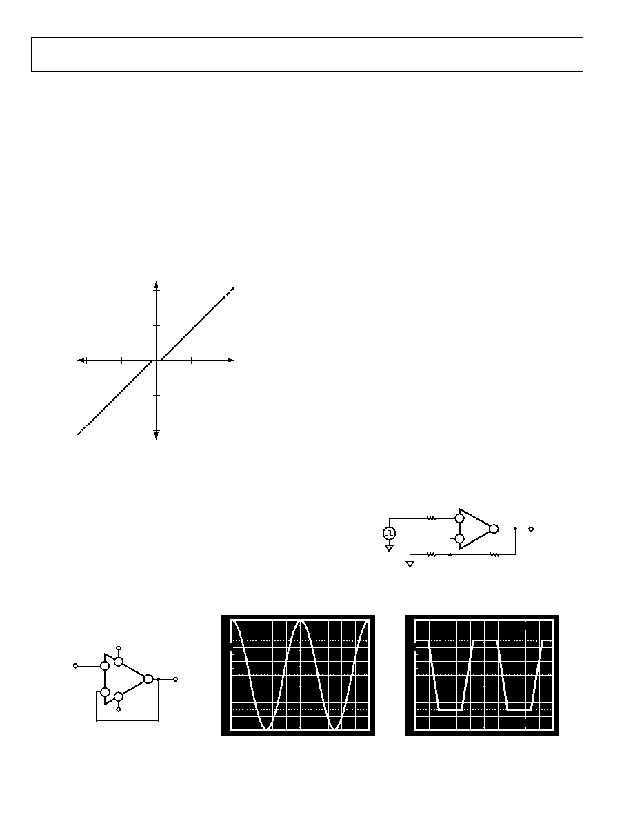
OVERDRIVE RECOVERY
The overdrive recovery time of an operational amplifier is the
time required for the output voltage to recover to its linear
region from a saturated condition. This recovery time is
important in applications where the amplifier must recover
quickly after a large transient event, such as a comparator. The
circuit shown in Figure 63 was used to evaluate the OPx91
overdrive recovery time. The OPx91 takes approximately 8 μs to
recover from positive saturation and approximately 6.5 μs to
recover from negative saturation.
+
–
1/2
OP291
3
2
1
R1
9k
R2
10k
R3
10k
VIN
10V STEP
VS = ±5V
VOUT
00
29
4-
06
8
Figure 63. Overdrive Recovery Time Test Circuit
10
90
100
0%
TIME (200s/DIV)
V
IN
(
2.
5V/
D
IV)
10
90
100
0%
TIME (200s/DIV)
V
OU
T
(2
V
/D
IV
)
20mV
5s
+5V
–5V
VIN
20V p-p
VOUT
8
1
3
2
4
1/2
OP291
+
–
00
29
4-
06
7
Figure 64. Output Voltage Phase Reversal Behavior
相关PDF资料 |
PDF描述 |
|---|---|
| AD626ARZ-REEL7 | IC AMP DIFF LP 12MA 8SOIC |
| PEC32SFAN | CONN HEADER .100 SINGL STR 32POS |
| LT1228CS8#PBF | IC CURRNT FEEDBK AMP 100MHZ8SOIC |
| 71764-0018 | CONN HDR DUAL 18POS .100 R/A TIN |
| LT1058CN#PBF | IC PREC OP-AMP JFET QUAD 14-DIP |
相关代理商/技术参数 |
参数描述 |
|---|---|
| OP491GPZ | 制造商:Analog Devices 功能描述:Operational Amplifier (Op-Amp) IC |
| OP491GRU | 制造商:未知厂家 制造商全称:未知厂家 功能描述:OP-AMP|QUAD|BICMOS|TSSOP|14PIN|PLASTIC |
| OP491GRU-REEL | 功能描述:IC OPAMP GP R-R 3MHZ 14TSSOP RoHS:否 类别:集成电路 (IC) >> Linear - Amplifiers - Instrumentation 系列:- 标准包装:2,500 系列:- 放大器类型:通用 电路数:1 输出类型:满摆幅 转换速率:0.11 V/µs 增益带宽积:350kHz -3db带宽:- 电流 - 输入偏压:4nA 电压 - 输入偏移:20µV 电流 - 电源:260µA 电流 - 输出 / 通道:20mA 电压 - 电源,单路/双路(±):2.7 V ~ 36 V,±1.35 V ~ 18 V 工作温度:-40°C ~ 85°C 安装类型:表面贴装 封装/外壳:8-SOIC(0.154",3.90mm 宽) 供应商设备封装:8-SO 包装:带卷 (TR) |
| OP491GRUZ-REEL | 功能描述:IC OPAMP GP R-R 3MHZ 14TSSOP RoHS:是 类别:集成电路 (IC) >> Linear - Amplifiers - Instrumentation 系列:- 产品培训模块:Differential Circuit Design Techniques for Communication Applications 标准包装:1 系列:- 放大器类型:RF/IF 差分 电路数:1 输出类型:差分 转换速率:9800 V/µs 增益带宽积:- -3db带宽:2.9GHz 电流 - 输入偏压:3µA 电压 - 输入偏移:- 电流 - 电源:40mA 电流 - 输出 / 通道:- 电压 - 电源,单路/双路(±):3 V ~ 3.6 V 工作温度:-40°C ~ 85°C 安装类型:表面贴装 封装/外壳:16-VQFN 裸露焊盘,CSP 供应商设备封装:16-LFCSP-VQ 包装:剪切带 (CT) 产品目录页面:551 (CN2011-ZH PDF) 其它名称:ADL5561ACPZ-R7CT |
| OP491GS | 功能描述:IC OPAMP GP R-R 3MHZ QUAD 14SOIC RoHS:否 类别:集成电路 (IC) >> Linear - Amplifiers - Instrumentation 系列:- 标准包装:2,500 系列:- 放大器类型:通用 电路数:1 输出类型:满摆幅 转换速率:0.11 V/µs 增益带宽积:350kHz -3db带宽:- 电流 - 输入偏压:4nA 电压 - 输入偏移:20µV 电流 - 电源:260µA 电流 - 输出 / 通道:20mA 电压 - 电源,单路/双路(±):2.7 V ~ 36 V,±1.35 V ~ 18 V 工作温度:-40°C ~ 85°C 安装类型:表面贴装 封装/外壳:8-SOIC(0.154",3.90mm 宽) 供应商设备封装:8-SO 包装:带卷 (TR) |
发布紧急采购,3分钟左右您将得到回复。