参数资料
| 型号: | OP491GPZ |
| 厂商: | Analog Devices Inc |
| 文件页数: | 11/24页 |
| 文件大小: | 0K |
| 描述: | IC OPAMP GP R-R 3MHZ QUAD 14DIP |
| 标准包装: | 25 |
| 放大器类型: | 通用 |
| 电路数: | 4 |
| 输出类型: | 满摆幅 |
| 转换速率: | 0.5 V/µs |
| 增益带宽积: | 3MHz |
| 电流 - 输入偏压: | 30nA |
| 电压 - 输入偏移: | 80µV |
| 电流 - 电源: | 260µA |
| 电流 - 输出 / 通道: | 16mA |
| 电压 - 电源,单路/双路(±): | 2.7 V ~ 12 V,±1.35 V ~ 6 V |
| 工作温度: | -40°C ~ 125°C |
| 安装类型: | 通孔 |
| 封装/外壳: | 14-DIP(0.300",7.62mm) |
| 供应商设备封装: | 14-PDIP |
| 包装: | 管件 |
| 产品目录页面: | 774 (CN2011-ZH PDF) |
OP191/OP291/OP491
Rev. E | Page 19 of 24
APPLICATIONS INFORMATION
SINGLE 3 V SUPPLY, INSTRUMENTATION
AMPLIFIER
The OP291 low supply current and low voltage operation
make it ideal for battery-powered applications, such as the
instrumentation amplifier shown in Figure 65. The circuit uses
the classic two op amp instrumentation amplifier topology, with
four resistors to set the gain. The equation is simply that of a
noninverting amplifier, as shown in Figure 65. The two resistors
labeled R1 should be closely matched both to each other and to
the two resistors labeled R2 to ensure good common-mode
rejection performance. Resistor networks ensure the closest
matching as well as matched drifts for good temperature
stability. Capacitor C1 is included to limit the bandwidth and,
therefore, the noise in sensitive applications. The value of this
capacitor should be adjusted depending on the desired closed-
loop bandwidth of the instrumentation amplifier. The RC
combination creates a pole at a frequency equal to 1/(2π ×
R1C1). If AC-CMRR is critical, then a matched capacitor to C1
should be included across the second resistor labeled R1.
1/2
OP291
1/2
OP291
R1
R2
R1
3V
C1
100pF
VIN
VOUT
VOUT = (1 +
) = VIN
R1
R2
–
00
29
4-
0
69
3
2
1
8
5
6
4
7
+
Figure 65. Single 3 V Supply Instrumentation Amplifier
Because the OP291 accepts rail-to-rail inputs, the input
common-mode range includes both ground and the positive
supply of 3 V. Furthermore, the rail-to-rail output range ensures
the widest signal range possible and maximizes the dynamic
range of the system. Also, with its low supply current of
300 μA/device, this circuit consumes a quiescent current of
only 600 μA yet still exhibits a gain bandwidth of 3 MHz.
A question may arise about other instrumentation amplifier
topologies for single-supply applications. For example, a
variation on this topology adds a fifth resistor between the two
inverting inputs of the op amps for gain setting. While that
topology works well in dual-supply applications, it is inherently
inappropriate for single-supply circuits. The same could be said
for the traditional three op amp instrumentation amplifier. In
both cases, the circuits simply cannot work in single-supply
situations unless a false ground between the supplies is created.
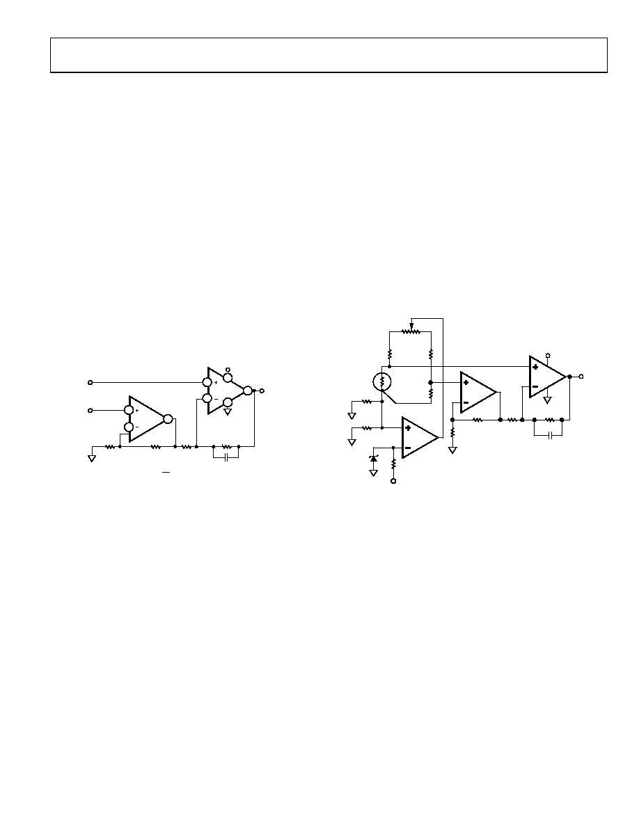
SINGLE-SUPPLY RTD AMPLIFIER
The circuit in Figure 66 uses three op amps of the OP491 to
develop a bridge configuration for an RTD amplifier that
operates from a single 5 V supply. The circuit takes advantage of
the OP491 wide output swing range to generate a high bridge
excitation voltage of 3.9 V. In fact, because of the rail-to-rail
output swing, this circuit works with supplies as low as 4.0 V.
Amplifier A1 servos the bridge to create a constant excitation
current in conjunction with the AD589, a 1.235 V precision
reference. The op amp maintains the reference voltage across
the parallel combination of the 6.19 kΩ and 2.55 MΩ resistors,
which generate a 200 μA current source. This current splits
evenly and flows through both halves of the bridge. Thus,
100 μA flows through the RTD to generate an output voltage
based on its resistance. A 3-wire RTD is used to balance the line
resistance in both 100 Ω legs of the bridge to improve accuracy.
1/4
OP491
VOUT
365
1/4
OP491
100k
0.01pF
A3
5V
GAIN = 274
100k
1/4
OP491
37.4k
5V
AD589
2.55M
6.19k
200
10 TURNS
26.7k
A2
A1
100
RTD
ALL RESISTORS 1% OR BETTER
00
29
4-
0
70
Figure 66. Single-Supply RTD Amplifier
Amplifier A2 and Amplifier A3 are configured in the two op
amp instrumentation amplifier topology described in the Single
3 V Supply, Instrumentation Amplifier section. The resistors are
chosen to produce a gain of 274, such that each 1°C increase in
temperature results in a 10 mV change in the output voltage, for
ease of measurement. A 0.01 μF capacitor is included in parallel
with the 100 kΩ resistor on Amplifier A3 to filter out any
unwanted noise from this high gain circuit. This particular RC
combination creates a pole at 1.6 kHz.
相关PDF资料 |
PDF描述 |
|---|---|
| AD626ARZ-REEL7 | IC AMP DIFF LP 12MA 8SOIC |
| PEC32SFAN | CONN HEADER .100 SINGL STR 32POS |
| LT1228CS8#PBF | IC CURRNT FEEDBK AMP 100MHZ8SOIC |
| 71764-0018 | CONN HDR DUAL 18POS .100 R/A TIN |
| LT1058CN#PBF | IC PREC OP-AMP JFET QUAD 14-DIP |
相关代理商/技术参数 |
参数描述 |
|---|---|
| OP491GPZ | 制造商:Analog Devices 功能描述:Operational Amplifier (Op-Amp) IC |
| OP491GRU | 制造商:未知厂家 制造商全称:未知厂家 功能描述:OP-AMP|QUAD|BICMOS|TSSOP|14PIN|PLASTIC |
| OP491GRU-REEL | 功能描述:IC OPAMP GP R-R 3MHZ 14TSSOP RoHS:否 类别:集成电路 (IC) >> Linear - Amplifiers - Instrumentation 系列:- 标准包装:2,500 系列:- 放大器类型:通用 电路数:1 输出类型:满摆幅 转换速率:0.11 V/µs 增益带宽积:350kHz -3db带宽:- 电流 - 输入偏压:4nA 电压 - 输入偏移:20µV 电流 - 电源:260µA 电流 - 输出 / 通道:20mA 电压 - 电源,单路/双路(±):2.7 V ~ 36 V,±1.35 V ~ 18 V 工作温度:-40°C ~ 85°C 安装类型:表面贴装 封装/外壳:8-SOIC(0.154",3.90mm 宽) 供应商设备封装:8-SO 包装:带卷 (TR) |
| OP491GRUZ-REEL | 功能描述:IC OPAMP GP R-R 3MHZ 14TSSOP RoHS:是 类别:集成电路 (IC) >> Linear - Amplifiers - Instrumentation 系列:- 产品培训模块:Differential Circuit Design Techniques for Communication Applications 标准包装:1 系列:- 放大器类型:RF/IF 差分 电路数:1 输出类型:差分 转换速率:9800 V/µs 增益带宽积:- -3db带宽:2.9GHz 电流 - 输入偏压:3µA 电压 - 输入偏移:- 电流 - 电源:40mA 电流 - 输出 / 通道:- 电压 - 电源,单路/双路(±):3 V ~ 3.6 V 工作温度:-40°C ~ 85°C 安装类型:表面贴装 封装/外壳:16-VQFN 裸露焊盘,CSP 供应商设备封装:16-LFCSP-VQ 包装:剪切带 (CT) 产品目录页面:551 (CN2011-ZH PDF) 其它名称:ADL5561ACPZ-R7CT |
| OP491GS | 功能描述:IC OPAMP GP R-R 3MHZ QUAD 14SOIC RoHS:否 类别:集成电路 (IC) >> Linear - Amplifiers - Instrumentation 系列:- 标准包装:2,500 系列:- 放大器类型:通用 电路数:1 输出类型:满摆幅 转换速率:0.11 V/µs 增益带宽积:350kHz -3db带宽:- 电流 - 输入偏压:4nA 电压 - 输入偏移:20µV 电流 - 电源:260µA 电流 - 输出 / 通道:20mA 电压 - 电源,单路/双路(±):2.7 V ~ 36 V,±1.35 V ~ 18 V 工作温度:-40°C ~ 85°C 安装类型:表面贴装 封装/外壳:8-SOIC(0.154",3.90mm 宽) 供应商设备封装:8-SO 包装:带卷 (TR) |
发布紧急采购,3分钟左右您将得到回复。