- 您现在的位置:买卖IC网 > PDF目录268233 > OR2C26A4BA352-DB (LATTICE SEMICONDUCTOR CORP) FPGA, 576 CLBS, 27600 GATES, PBGA352 PDF资料下载
参数资料
| 型号: | OR2C26A4BA352-DB |
| 厂商: | LATTICE SEMICONDUCTOR CORP |
| 元件分类: | FPGA |
| 英文描述: | FPGA, 576 CLBS, 27600 GATES, PBGA352 |
| 封装: | PLASTIC, BGA-352 |
| 文件页数: | 131/196页 |
| 文件大小: | 3475K |
| 代理商: | OR2C26A4BA352-DB |
第1页第2页第3页第4页第5页第6页第7页第8页第9页第10页第11页第12页第13页第14页第15页第16页第17页第18页第19页第20页第21页第22页第23页第24页第25页第26页第27页第28页第29页第30页第31页第32页第33页第34页第35页第36页第37页第38页第39页第40页第41页第42页第43页第44页第45页第46页第47页第48页第49页第50页第51页第52页第53页第54页第55页第56页第57页第58页第59页第60页第61页第62页第63页第64页第65页第66页第67页第68页第69页第70页第71页第72页第73页第74页第75页第76页第77页第78页第79页第80页第81页第82页第83页第84页第85页第86页第87页第88页第89页第90页第91页第92页第93页第94页第95页第96页第97页第98页第99页第100页第101页第102页第103页第104页第105页第106页第107页第108页第109页第110页第111页第112页第113页第114页第115页第116页第117页第118页第119页第120页第121页第122页第123页第124页第125页第126页第127页第128页第129页第130页当前第131页第132页第133页第134页第135页第136页第137页第138页第139页第140页第141页第142页第143页第144页第145页第146页第147页第148页第149页第150页第151页第152页第153页第154页第155页第156页第157页第158页第159页第160页第161页第162页第163页第164页第165页第166页第167页第168页第169页第170页第171页第172页第173页第174页第175页第176页第177页第178页第179页第180页第181页第182页第183页第184页第185页第186页第187页第188页第189页第190页第191页第192页第193页第194页第195页第196页
Data Sheet
ORCA Series 2 FPGAs
January 2003
4
Lattice Semiconductor
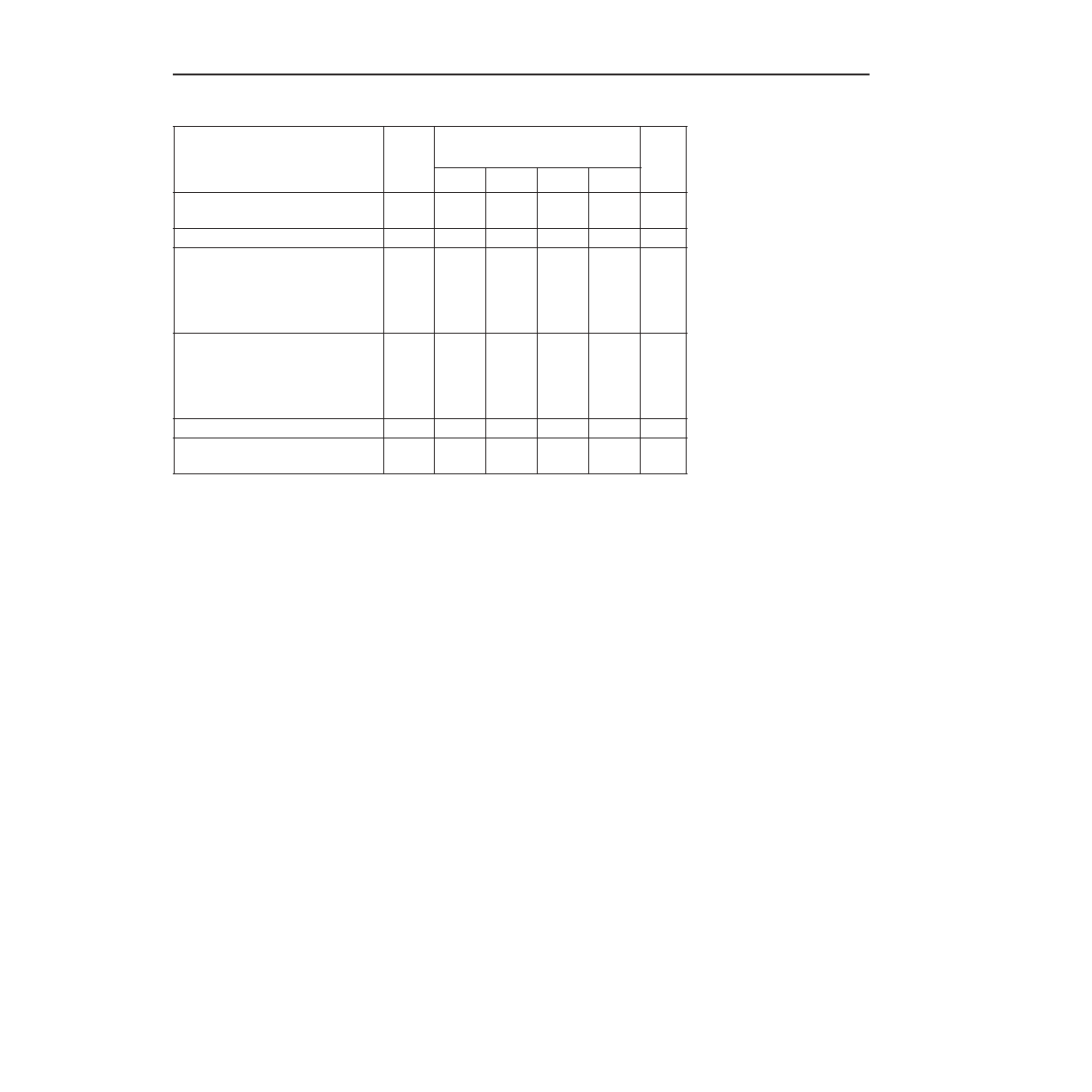
Table 3. ORCA Series 2TA System Performance
1.Implemented using 4 x 1 multiplier mode (unpipelined), register-to-register, two 8-bit inputs, one 16-bit output.
2. Implemented using two 16 x 12 ROMs and one 12-bit adder, one 8-bit input, one xed operand, one 16-bit output.
3. Implemented using 4 x 1 multiplier mode (fully pipelined), two 8-bit inputs, one 16-bit output (28 of 44 PFUs contain only pipelining registers).
4. Implemented using 16 x 4 synchronous single-port RAM mode allowing both read and write per clock cycle, including write/read address
multiplexer.
5. Implemented using 16 x 4 synchronous single-port RAM mode allowing either read or write per clock cycle, including write/read address mul-
tiplexer.
6. Implemented using 16 x 2 synchronous dual-port RAM mode.
Function
#
PFUs
Speed Grade
Unit
-4
-5
-6
-7
16-bit loadable up/down
counter
4
87.0
104.2
129.9
144.9
MHz
16-bit accumulator
4
87.0
104.2
129.9
144.9
MHz
8 x 8 parallel multiplier:
— Multiplier mode,
unpipelined1
— ROM mode, unpipelined2
— Multiplier mode, pipelined3
22
9
44
25.1
71.9
82.0
31.0
87.7
103.1
36.0
107.5
125.0
40.3
122.0
142.9
MHz
32 x 16 RAM:
— Single port (read and write/
cycle)4
— Single port5
— Dual port6
9
16
36.2
69.0
83.3
53.8
92.6
53.8
92.6
62.5
96.2
MHz
36-bit parity check (internal)
4
9.1
7.4
5.6
5.2
ns
32-bit address decode
(internal)
3.25
7.5
6.1
4.6
4.3
ns
相关PDF资料 |
PDF描述 |
|---|---|
| OR2C26A4BC432-DB | FPGA, 576 CLBS, 27600 GATES, PBGA432 |
| OR2T10A4BA352-DB | FPGA, 256 CLBS, 12300 GATES, PBGA352 |
| OR2T10A4BA352I-DB | FPGA, 256 CLBS, 12300 GATES, PBGA352 |
| OR2T10A4J160I-DB | FPGA, 256 CLBS, 12300 GATES, PQFP160 |
| OR2T10A4S240-DB | FPGA, 256 CLBS, 12300 GATES, PQFP240 |
相关代理商/技术参数 |
参数描述 |
|---|---|
| OR2C26A-4PS208 | 制造商:Lattice Semiconductor Corporation 功能描述:FPGA, 576 CLBS, 27600 GATES, PQFP208 |
| OR2C26A4PS208-DB | 功能描述:FPGA - 现场可编程门阵列 2304 LUT 342 I/O RoHS:否 制造商:Altera Corporation 系列:Cyclone V E 栅极数量: 逻辑块数量:943 内嵌式块RAM - EBR:1956 kbit 输入/输出端数量:128 最大工作频率:800 MHz 工作电源电压:1.1 V 最大工作温度:+ 70 C 安装风格:SMD/SMT 封装 / 箱体:FBGA-256 |
| OR2C26A4PS208I-DB | 功能描述:FPGA - 现场可编程门阵列 Use ECP/EC or XP RoHS:否 制造商:Altera Corporation 系列:Cyclone V E 栅极数量: 逻辑块数量:943 内嵌式块RAM - EBR:1956 kbit 输入/输出端数量:128 最大工作频率:800 MHz 工作电源电压:1.1 V 最大工作温度:+ 70 C 安装风格:SMD/SMT 封装 / 箱体:FBGA-256 |
| OR2C26A4PS240-DB | 功能描述:FPGA - 现场可编程门阵列 Use ECP/EC or XP RoHS:否 制造商:Altera Corporation 系列:Cyclone V E 栅极数量: 逻辑块数量:943 内嵌式块RAM - EBR:1956 kbit 输入/输出端数量:128 最大工作频率:800 MHz 工作电源电压:1.1 V 最大工作温度:+ 70 C 安装风格:SMD/SMT 封装 / 箱体:FBGA-256 |
| OR2C26A4PS304-DB | 功能描述:FPGA - 现场可编程门阵列 Use ECP/EC or XP RoHS:否 制造商:Altera Corporation 系列:Cyclone V E 栅极数量: 逻辑块数量:943 内嵌式块RAM - EBR:1956 kbit 输入/输出端数量:128 最大工作频率:800 MHz 工作电源电压:1.1 V 最大工作温度:+ 70 C 安装风格:SMD/SMT 封装 / 箱体:FBGA-256 |
发布紧急采购,3分钟左右您将得到回复。