- 您现在的位置:买卖IC网 > PDF目录268233 > OR2T04A4J160I-DB (LATTICE SEMICONDUCTOR CORP) FPGA, 100 CLBS, 4800 GATES, PQFP160 PDF资料下载
参数资料
| 型号: | OR2T04A4J160I-DB |
| 厂商: | LATTICE SEMICONDUCTOR CORP |
| 元件分类: | FPGA |
| 英文描述: | FPGA, 100 CLBS, 4800 GATES, PQFP160 |
| 封装: | QFP-160 |
| 文件页数: | 132/196页 |
| 文件大小: | 3475K |
| 代理商: | OR2T04A4J160I-DB |
第1页第2页第3页第4页第5页第6页第7页第8页第9页第10页第11页第12页第13页第14页第15页第16页第17页第18页第19页第20页第21页第22页第23页第24页第25页第26页第27页第28页第29页第30页第31页第32页第33页第34页第35页第36页第37页第38页第39页第40页第41页第42页第43页第44页第45页第46页第47页第48页第49页第50页第51页第52页第53页第54页第55页第56页第57页第58页第59页第60页第61页第62页第63页第64页第65页第66页第67页第68页第69页第70页第71页第72页第73页第74页第75页第76页第77页第78页第79页第80页第81页第82页第83页第84页第85页第86页第87页第88页第89页第90页第91页第92页第93页第94页第95页第96页第97页第98页第99页第100页第101页第102页第103页第104页第105页第106页第107页第108页第109页第110页第111页第112页第113页第114页第115页第116页第117页第118页第119页第120页第121页第122页第123页第124页第125页第126页第127页第128页第129页第130页第131页当前第132页第133页第134页第135页第136页第137页第138页第139页第140页第141页第142页第143页第144页第145页第146页第147页第148页第149页第150页第151页第152页第153页第154页第155页第156页第157页第158页第159页第160页第161页第162页第163页第164页第165页第166页第167页第168页第169页第170页第171页第172页第173页第174页第175页第176页第177页第178页第179页第180页第181页第182页第183页第184页第185页第186页第187页第188页第189页第190页第191页第192页第193页第194页第195页第196页
40
Lattice Semiconductor
Data Sheet
ORCA Series 2 FPGAs
January 2003
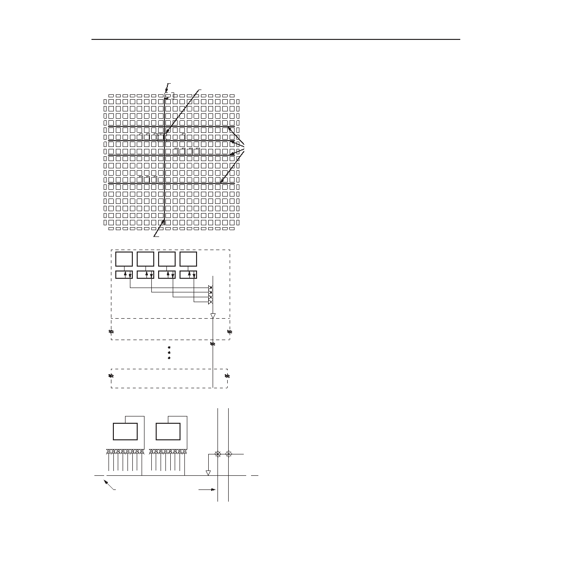
Clock Distribution Network (continued)
5-4480(F).r3
Figure 34. Primary Clock Distribution
Secondary Clock
There are times when a primary clock is either not
available or not desired, and a secondary clock is
needed. For example:
■
Only one input pad per PIC can be placed on the
clock routing. If a second input pad in a given PIC
requires global signal routing, a secondary clock
route must be used.
■
Since there is only one branch driver in each PLC for
either direction (vertical and horizontal), both clock
lines in a particular row or column (CKL and CKR, for
example) cannot drive a branch. Therefore, two
clocks should not be placed into I/O pads in PICs on
the opposite sides of the same row or column if glo-
bal clocks are to be used.
■
Since the clock lines can only be driven from input
pads, internally generated clocks should use second-
ary clock routing.
Figure 35 illustrates the secondary clock distribution. If
the clock signal originates from either the left or right
side of the FPGA, it can be routed through the TRIDI
buffers in the PIC onto one of the adjacent PLC’s hori-
zontal XL lines. If the clock signal originates from the
top or bottom of the FPGA, the vertical XL lines are
used for routing. In either case, an XL line is used as
the clock spine. In the same manner, if a clock is only
going to be used in one quadrant, the XH lines can be
used as a clock spine. The routing of the clock spine
from the input pads to the VXL (VXH) using the BIDIs
(BIDIHs) is shown in Figure 35, Detail A.
In each PLC, a low-skew connection through a long-
line driver can be used to connect a horizontal XL line
to a vertical XL line or vice versa. As shown in Figure
35, Detail B, this is used to route the branches from the
clock spine. If the clock spine is a vertical XL line, then
the branches are horizontal XL lines and vice versa.
The clock is then routed into each PLC from the XL line
clock branches.
To minimize skew, the PLC clock input for all PLCs
must be connected to the branch XL lines, not the
spine XL line. Even in PLCs where the clock is routed
from the spine to the branches, the clock should be
routed back into the PLC from the clock branch.
If the clock is to drive only a limited number of loads,
the PFUs can be connected directly to the clock spine.
In this case, all ip-ops driven by the clock must be
located in the same row or column.
CKT
CKB
HXL
HCK
R7C8
HCK
DETAIL B
R7C7
HXL
CLOCK
BRANCH
CLOCK
SPINES
PLC R1C8
PLC R18C8
PIC PT8
CLOCK SPINE
CKT
DETAIL A
AB
C
D
CLOCK
CLOCK SPINE
SEE DETAIL A
SEE DETAIL B
CLK PIN
BRANCHES
DT
相关PDF资料 |
PDF描述 |
|---|---|
| OR2T04A4M84-D | FPGA, 100 CLBS, 4800 GATES, PQCC84 |
| OR2T04A4M84I-D | FPGA, 100 CLBS, 4800 GATES, PQCC84 |
| OR2T04A5J160-DB | FPGA, 100 CLBS, 4800 GATES, PQFP160 |
| OR2T04A5M84-D | FPGA, 100 CLBS, 4800 GATES, PQCC84 |
| OR2C26A3BA352I-DB | FPGA, 576 CLBS, 27600 GATES, PBGA352 |
相关代理商/技术参数 |
参数描述 |
|---|---|
| OR2T04A-4J208 | 制造商:未知厂家 制造商全称:未知厂家 功能描述:Field-Programmable Gate Arrays |
| OR2T04A-4J208I | 制造商:未知厂家 制造商全称:未知厂家 功能描述:Field-Programmable Gate Arrays |
| OR2T04A-4J84 | 制造商:未知厂家 制造商全称:未知厂家 功能描述:Field-Programmable Gate Arrays |
| OR2T04A-4J84I | 制造商:未知厂家 制造商全称:未知厂家 功能描述:Field-Programmable Gate Arrays |
| OR2T04A-4M100 | 制造商:未知厂家 制造商全称:未知厂家 功能描述:Field-Programmable Gate Arrays |
发布紧急采购,3分钟左右您将得到回复。