- 您现在的位置:买卖IC网 > PDF目录189437 > OR2T26A-6S432 (Electronic Theatre Controls, Inc.) Field-Programmable Gate Arrays PDF资料下载
参数资料
| 型号: | OR2T26A-6S432 |
| 厂商: | Electronic Theatre Controls, Inc. |
| 元件分类: | FPGA |
| 英文描述: | Field-Programmable Gate Arrays |
| 中文描述: | 现场可编程门阵列 |
| 文件页数: | 126/192页 |
| 文件大小: | 3148K |
| 代理商: | OR2T26A-6S432 |
第1页第2页第3页第4页第5页第6页第7页第8页第9页第10页第11页第12页第13页第14页第15页第16页第17页第18页第19页第20页第21页第22页第23页第24页第25页第26页第27页第28页第29页第30页第31页第32页第33页第34页第35页第36页第37页第38页第39页第40页第41页第42页第43页第44页第45页第46页第47页第48页第49页第50页第51页第52页第53页第54页第55页第56页第57页第58页第59页第60页第61页第62页第63页第64页第65页第66页第67页第68页第69页第70页第71页第72页第73页第74页第75页第76页第77页第78页第79页第80页第81页第82页第83页第84页第85页第86页第87页第88页第89页第90页第91页第92页第93页第94页第95页第96页第97页第98页第99页第100页第101页第102页第103页第104页第105页第106页第107页第108页第109页第110页第111页第112页第113页第114页第115页第116页第117页第118页第119页第120页第121页第122页第123页第124页第125页当前第126页第127页第128页第129页第130页第131页第132页第133页第134页第135页第136页第137页第138页第139页第140页第141页第142页第143页第144页第145页第146页第147页第148页第149页第150页第151页第152页第153页第154页第155页第156页第157页第158页第159页第160页第161页第162页第163页第164页第165页第166页第167页第168页第169页第170页第171页第172页第173页第174页第175页第176页第177页第178页第179页第180页第181页第182页第183页第184页第185页第186页第187页第188页第189页第190页第191页第192页
Lucent Technologies Inc.
39
Data Sheet
June 1999
ORCA Series 2 FPGAs
Clock Distribution Network (continued)
Alternatively, the clock can be routed from the spine to
the branches by using the BIDIs instead of the long-line
drivers. This results in added delay in the clock net, but
the clock skew is approximately equal to the clock
routed using the long-line drivers. This method can be
used to create a clock that is used in only one quad-
rant. The XH lines act as a clock spine, which is then
routed to perpendicular XH lines (the branches) using
the BIDIHs.
Clock signals, such as the output of a counter, can also
be generated in PLCs and routed onto an XL line,
which then acts as a clock spine. Although the clock
can be generated in any PLC, it is recommended that
the clock be located as close to the center of the FPGA
as possible to minimize clock skew.
Selecting Clock Input Pins
Any user I/O pin on an
ORCA FPGA can be used as a
very fast, low-skew clock input. Choosing the first clock
pin is completely arbitrary, but using a pin that is near
the center of an edge of the device (as shown in Fig-
ures 34 and 35) will provide the lowest skew clock net-
work. The pin-to-pin timing numbers in the Timing
Characteristics section of this data book assume that
the clock pin is in one of the four PICs at the center of
any side of the device.
Once the first clock pin has been chosen, there are
only two sets of pins (within the center four PICs on
each side of the device) that should not be chosen as
the second clock pin: a pin from the same PIC, and/or a
pin from the PIC on the exact opposite edge of the die
(i.e., if a pin from a PIC on the top edge is chosen for
the first clock, the same PIC on the bottom edge should
not be chosen for the second clock).
These rules should be followed iteratively until a total of
eight clocks (or other global signals) have been
selected: four from the left/right sides of the device, and
four from the top/bottom sides of the device. If more
than eight clocks are needed, then select another pin
outside the center four PICs to use primary-clock rout-
ing, use secondary clock routing for any pin, or use
local clock routing.
If it is desired to use a pin for one of the first eight
clocks that is not within the center four PICs of any side
of the device and primary clock routing is desired, the
pad names (see Pin Information) of the two clock pins
on the top or bottom of the device cannot be a multi-
plier of four PICs away. The same rule applies to clock
pins on the left or right side of the device.
The following equation can be used to determine pin
names:
Pad number = P[RL][TB]n ± (i x 4)[A – D]
Where i = 1—8, and n is the current PIC number.
For more information, please refer to
Utilizing the
ORCA
OR2C/TxxA Clock Distribution Network Appli-
cation Note (AP97-055FPGA).
5-4481(F).r2
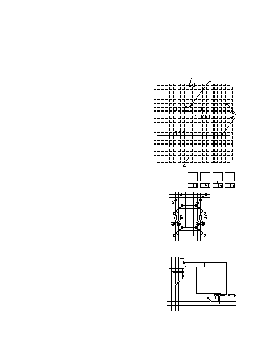
Figure 35. Secondary Clock Distribution
DT
CLOCK
CLOCK SPINE
SEE DETAIL A
SEE DETAIL B
CLK PIN
BRANCHES
PFU
HCK
VCK
DETAIL B
PA
PB
VXL[3]
VXL[2]
VXL[1]
VXL[0]
VXH[3]
VXH[2]
VXH[1]
VXH[0]
DETAIL A
PC
PD
相关PDF资料 |
PDF描述 |
|---|---|
| OR2T26A-6S432I | Field-Programmable Gate Arrays |
| OR2T26A-6T208 | Field-Programmable Gate Arrays |
| OR2T26A-6T208I | Field-Programmable Gate Arrays |
| OR2T26A-6T240 | Field-Programmable Gate Arrays |
| OR2T26A-6T240I | Field-Programmable Gate Arrays |
相关代理商/技术参数 |
参数描述 |
|---|---|
| OR2T26A7BA352-DB | 功能描述:FPGA - 现场可编程门阵列 2304 LUT 326 I/O RoHS:否 制造商:Altera Corporation 系列:Cyclone V E 栅极数量: 逻辑块数量:943 内嵌式块RAM - EBR:1956 kbit 输入/输出端数量:128 最大工作频率:800 MHz 工作电源电压:1.1 V 最大工作温度:+ 70 C 安装风格:SMD/SMT 封装 / 箱体:FBGA-256 |
| OR2T26A7BC432-DB | 功能描述:FPGA - 现场可编程门阵列 2304 LUT 326 I/O RoHS:否 制造商:Altera Corporation 系列:Cyclone V E 栅极数量: 逻辑块数量:943 内嵌式块RAM - EBR:1956 kbit 输入/输出端数量:128 最大工作频率:800 MHz 工作电源电压:1.1 V 最大工作温度:+ 70 C 安装风格:SMD/SMT 封装 / 箱体:FBGA-256 |
| OR2T26A7PS208-DB | 功能描述:FPGA - 现场可编程门阵列 2304 LUT 326 I/O RoHS:否 制造商:Altera Corporation 系列:Cyclone V E 栅极数量: 逻辑块数量:943 内嵌式块RAM - EBR:1956 kbit 输入/输出端数量:128 最大工作频率:800 MHz 工作电源电压:1.1 V 最大工作温度:+ 70 C 安装风格:SMD/SMT 封装 / 箱体:FBGA-256 |
| OR2T26A7PS240-DB | 功能描述:FPGA - 现场可编程门阵列 2304 LUT 326 I/O RoHS:否 制造商:Altera Corporation 系列:Cyclone V E 栅极数量: 逻辑块数量:943 内嵌式块RAM - EBR:1956 kbit 输入/输出端数量:128 最大工作频率:800 MHz 工作电源电压:1.1 V 最大工作温度:+ 70 C 安装风格:SMD/SMT 封装 / 箱体:FBGA-256 |
| OR2T26A7S208-DB | 功能描述:FPGA - 现场可编程门阵列 Use LatticeEC RoHS:否 制造商:Altera Corporation 系列:Cyclone V E 栅极数量: 逻辑块数量:943 内嵌式块RAM - EBR:1956 kbit 输入/输出端数量:128 最大工作频率:800 MHz 工作电源电压:1.1 V 最大工作温度:+ 70 C 安装风格:SMD/SMT 封装 / 箱体:FBGA-256 |
发布紧急采购,3分钟左右您将得到回复。