- 您现在的位置:买卖IC网 > PDF目录189449 > OR4E061BA352-DB (LATTICE SEMICONDUCTOR CORP) FPGA, 2024 CLBS, 515000 GATES, PBGA352 PDF资料下载
参数资料
| 型号: | OR4E061BA352-DB |
| 厂商: | LATTICE SEMICONDUCTOR CORP |
| 元件分类: | FPGA |
| 英文描述: | FPGA, 2024 CLBS, 515000 GATES, PBGA352 |
| 封装: | PLASTIC, BGA-352 |
| 文件页数: | 65/151页 |
| 文件大小: | 2680K |
| 代理商: | OR4E061BA352-DB |
第1页第2页第3页第4页第5页第6页第7页第8页第9页第10页第11页第12页第13页第14页第15页第16页第17页第18页第19页第20页第21页第22页第23页第24页第25页第26页第27页第28页第29页第30页第31页第32页第33页第34页第35页第36页第37页第38页第39页第40页第41页第42页第43页第44页第45页第46页第47页第48页第49页第50页第51页第52页第53页第54页第55页第56页第57页第58页第59页第60页第61页第62页第63页第64页当前第65页第66页第67页第68页第69页第70页第71页第72页第73页第74页第75页第76页第77页第78页第79页第80页第81页第82页第83页第84页第85页第86页第87页第88页第89页第90页第91页第92页第93页第94页第95页第96页第97页第98页第99页第100页第101页第102页第103页第104页第105页第106页第107页第108页第109页第110页第111页第112页第113页第114页第115页第116页第117页第118页第119页第120页第121页第122页第123页第124页第125页第126页第127页第128页第129页第130页第131页第132页第133页第134页第135页第136页第137页第138页第139页第140页第141页第142页第143页第144页第145页第146页第147页第148页第149页第150页第151页
20
Lattice Semiconductor
Data Sheet
September, 2002
ORCA Series 4 FPGAs
Programmable Logic Cells (continued)
5-5749(F)
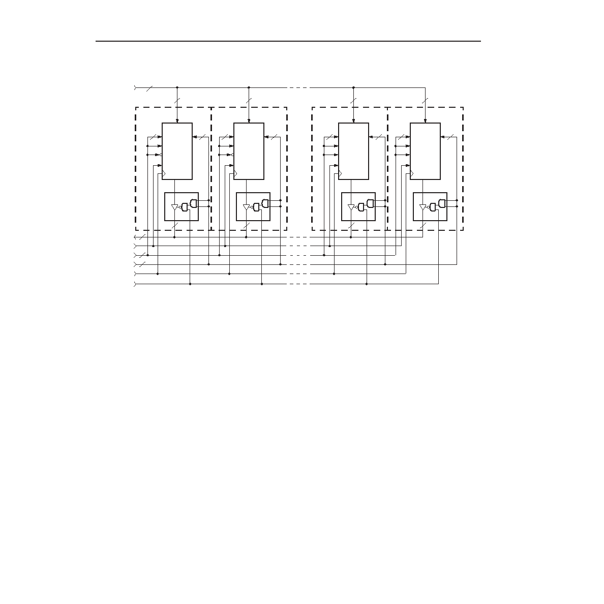
Figure 13. Memory Mode Expansion Example—128x8 RAM
RD[7:0]
WE
WA[6:0]
RA[6:0]
CLK
WA
RA
WPE 1
WPE 2
WE
WD[7:4]
5
4
PLC
8
WD[7:0]
8
7
WA
RA
WPE 1
WPE 2
WE
RD[3:0]
WD[3:0]
5
4
PLC
RD[7:4]
WA
RA
WPE 1
WPE 2
WE
WD[7:4]
5
4
PLC
WA
RA
WPE 1
WPE 2
WE
RD[3:0]
WD[3:0]
5
4
PLC
RD[7:4]
RE
4
RE
4
RE
4
RE
4
Supplemental Logic and Interconnect Cell
Each PLC contains a SLIC embedded within the PLC
routing, outside of the PFU. As its name indicates, the
SLIC performs both logic and interconnect (routing)
functions. Its main features are 3-statable, bidirectional
buffers, and a PAL-like decoder capability. Figure 14
shows a diagram of a SLIC with all of its features
shown. All modes of the SLIC are not available at one
time.
The ten SLIC inputs can be sourced directly from the
PFU or from the general routing fabric. SI[0:9] inputs
can come from the horizontal or vertical routing and
I[0:9} comes from the PFU outputs O[9:0]. These inputs
can also be tied to a logical 1 or 0 constant. The inputs
are twin-quad in nature and are segregated into two
groups of four nibbles and a third group of two inputs
for control. Each input nibble groups also have
3-state capability, however the third pair does not.
There is one 3-state control (TRI) for each SLIC, with
the capability to invert or disable the 3-state control for
each group of four BIDIs. Separate 3-state control for
each nibble-wide group is achievable by using the
SLICs decoder (DEC) output, driven by the group of
two BIDIs, to control the 3-state of one BIDI nibble
while using the TRI signal to control the 3-state of the
other BIDI nibble. Figure 15 shows the SLIC in buffer
mode with available 3-state control from the TRI and
DEC signals. If the entire SLIC is acting in a buffer
capacity, the DEC output may be used to generate a
constant logic 1 (VHI) or logic 0 (VLO) signal for general
use.
The SLIC may also be used to generate PAL-like AND-
OR with optional INVERT (AOI) functions or a decoder
of up to 10 bits. Each group of buffers can feed into an
AND gate (4-input AND for the nibble groups and
2-input AND for the other two buffers). These AND
gates then feed into a 3-input gate that can be cong-
ured as either an AND gate or an OR gate. The output
of the 3-input gate is invertible and is output at the DEC
output of the SLIC. Figure 19 shows the SLIC in full
decoder mode.
The functionality of the SLIC is parsed by the two nib-
ble-wide groups and the 2-bit buffer group. Each of
these groups may operate independently as BIDI buff-
ers (with or without 3-state capability for the nibble-
wide groups) or as a PAL/decoder.
相关PDF资料 |
PDF描述 |
|---|---|
| OR4E061BM680-DB | FPGA, 2024 CLBS, 515000 GATES, PBGA680 |
| OR4E062BA352-DB | FPGA, 2024 CLBS, 515000 GATES, PBGA352 |
| OR4E062BM680-DB | FPGA, 2024 CLBS, 515000 GATES, PBGA680 |
| OR4E063BA352-DB | FPGA, 2024 CLBS, 515000 GATES, PBGA352 |
| OR4E063BM680-DB | FPGA, 2024 CLBS, 515000 GATES, PBGA680 |
相关代理商/技术参数 |
参数描述 |
|---|---|
| OR4E06-1BA352I | 功能描述:FPGA - 现场可编程门阵列 16192 LUT 466 I/O RoHS:否 制造商:Altera Corporation 系列:Cyclone V E 栅极数量: 逻辑块数量:943 内嵌式块RAM - EBR:1956 kbit 输入/输出端数量:128 最大工作频率:800 MHz 工作电源电压:1.1 V 最大工作温度:+ 70 C 安装风格:SMD/SMT 封装 / 箱体:FBGA-256 |
| OR4E06-1BM680C | 功能描述:FPGA - 现场可编程门阵列 16192 LUT 466 I/O RoHS:否 制造商:Altera Corporation 系列:Cyclone V E 栅极数量: 逻辑块数量:943 内嵌式块RAM - EBR:1956 kbit 输入/输出端数量:128 最大工作频率:800 MHz 工作电源电压:1.1 V 最大工作温度:+ 70 C 安装风格:SMD/SMT 封装 / 箱体:FBGA-256 |
| OR4E06-1BM680I | 功能描述:FPGA - 现场可编程门阵列 16192 LUT 466 I/O RoHS:否 制造商:Altera Corporation 系列:Cyclone V E 栅极数量: 逻辑块数量:943 内嵌式块RAM - EBR:1956 kbit 输入/输出端数量:128 最大工作频率:800 MHz 工作电源电压:1.1 V 最大工作温度:+ 70 C 安装风格:SMD/SMT 封装 / 箱体:FBGA-256 |
| OR4E06-2BA352C | 功能描述:FPGA - 现场可编程门阵列 16192 LUT 466 I/O RoHS:否 制造商:Altera Corporation 系列:Cyclone V E 栅极数量: 逻辑块数量:943 内嵌式块RAM - EBR:1956 kbit 输入/输出端数量:128 最大工作频率:800 MHz 工作电源电压:1.1 V 最大工作温度:+ 70 C 安装风格:SMD/SMT 封装 / 箱体:FBGA-256 |
| OR4E06-2BM680C | 功能描述:FPGA - 现场可编程门阵列 16192 LUT 466 I/O RoHS:否 制造商:Altera Corporation 系列:Cyclone V E 栅极数量: 逻辑块数量:943 内嵌式块RAM - EBR:1956 kbit 输入/输出端数量:128 最大工作频率:800 MHz 工作电源电压:1.1 V 最大工作温度:+ 70 C 安装风格:SMD/SMT 封装 / 箱体:FBGA-256 |
发布紧急采购,3分钟左右您将得到回复。