- 您现在的位置:买卖IC网 > PDF目录189613 > P4C168L-35FSM (PYRAMID SEMICONDUCTOR CORP) 4K X 4 STANDARD SRAM, 35 ns, PDFP20 PDF资料下载
参数资料
| 型号: | P4C168L-35FSM |
| 厂商: | PYRAMID SEMICONDUCTOR CORP |
| 元件分类: | SRAM |
| 英文描述: | 4K X 4 STANDARD SRAM, 35 ns, PDFP20 |
| 封装: | DFP-20 |
| 文件页数: | 7/14页 |
| 文件大小: | 628K |
| 代理商: | P4C168L-35FSM |
P4C168/P4C168L, P4C169, P4C170
Page 2 of 14
Document # SRAM107 REV E
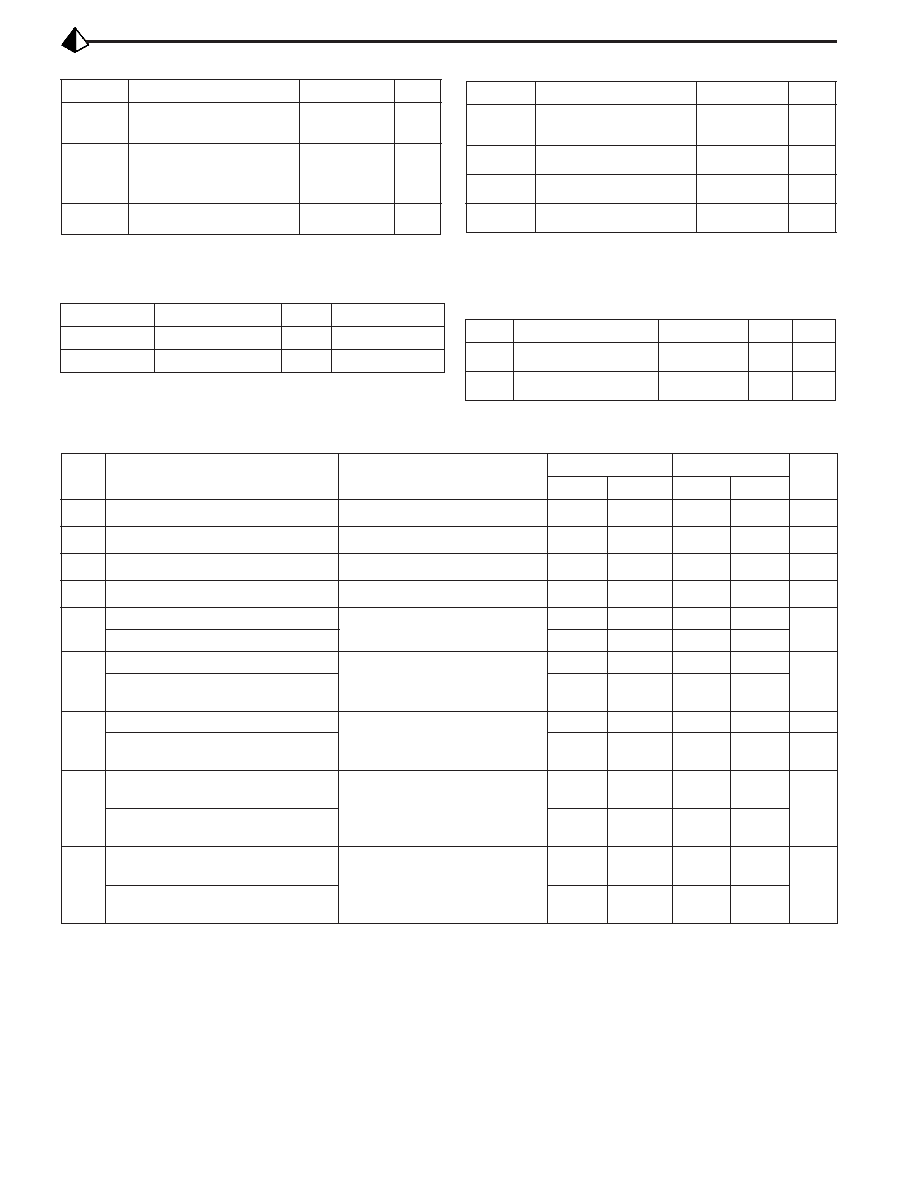
RECOMMENDED OPERATING CONDITIONS
CAPACITANCES(2)
(V
CC = 5.0V, TA = 25°C, f = 1.0MHz)
DC ELECTRICAL CHARACTERISTICS
MAxIMUM RATINGS(1)
Grade(2)
Ambient Temp
Gnd V
CC
Commercial 0°C to 70°C
0V
5.0V ± 10%
Military
-55°C to +125°C 0V
5.0V ± 10%
Symbol Parameter
Value
Unit
V
CC
Power Supply Pin with
Respect to GND
-0.5 to +7
V
TERM
Terminal Voltage with
respect to GND (up to
7.0V)
-0.5 to V
CC
+ 0.5
V
T
A
Operating Temperature -55 to +125
°C
Symbol Parameter
Value
Unit
T
BIAS
Temperature Under
Bias
-55 to +125 °C
T
STG
Storage Temperature -65 to +150 °C
P
T
Power Dissipation
1.0
W
I
OUT
DC Output Current
50
mA
Sym Parameter
Conditions Typ. Unit
C
IN
Input Capacitance
V
IN=0V
5
pF
C
OUT
Output Capacitance V
OUT=0V
7
pF
Sym Parameter
Test Conditions
P4C168/169/170
P4C168L
Unit
Min
Max
Min
Max
V
IH
Input High Voltage
2.2
V
CC+0.5
2.2
V
CC+0.5
V
IL
Input Low Voltage
-0.5(3)
0.8
-0.5(3)
0.8
V
OL
Output Low Voltage (TTL Load)
I
OL=+8 mA, VCC=Min
0.4
V
OH
Output High Voltage (TTL Load)
I
OH=-4 mA, VCC=Min
2.4
V
I
LI
Input Leakage Current (Military)
V
CC=Max, VIN=GND to VCC
-10
+10
-5
+5
A
Input Leakage Current (Commercial)
-5
+5
-2
+2
I
LO
Output Leakage Current (Military)
V
CC=Max, CS=VIH, VOUT=GND to
V
CC
-10
+10
-5
+5
A
Output Leakage Current (Commer-
cial)
-5
+5
-2
+2
I
CC
Dynamic Operating Current (Military)
V
CC=Max,f=Max, Outputs Open
—
120
—
120
mA
Dynamic Operating Current (Com-
mercial)
—
100
—
100
I
SB
Standby Power Supply Current (TTL
Input Levels) (Military)
CE
1≥VIH,VCC=Max,f=Max,Outputs
Open
—
40
—
40
mA
Standby Power Supply Current (TTL
Input Levels) (Commercial)
—
35
—
35
I
SB1
Standby Power Supply Current
(CMOS Input Levels) (Military)
CE
1≥VHC,VCC=Max,f=0,Outputs
Open,V
IN≤VLC or VIN≥VHC
—
20
—
1
mA
Standby Power Supply Current
(CMOS Input Levels) (Commercial)
—
15
—
0.2
Notes:
1. Stresses greater than those listed under MAXIMUM RATINGS may
cause permanent damage to the device. This is a stress rating only
and functional operation of the device at these or any other conditions
above those indicated in the operational sections of this specification
is not implied. Exposure to MAXIMUM rating conditions for extended
periods may affect reliability..
2. This parameter is sampled and not 100% tested.
3. Transient inputs with V
IL and IIL not more negative than -3.0V and -100mA,
respectively, are permissible for pulse widths up to 20 ns.
相关PDF资料 |
PDF描述 |
|---|---|
| P4C180-15PC | 4K X 4 CACHE TAG SRAM, 15 ns, PDIP22 |
| P4C198A-20CC | x4 SRAM |
| P4C198A-20JC | x4 SRAM |
| P4C198A-20LC | x4 SRAM |
| P4C198L-35PC | x4 SRAM |
相关代理商/技术参数 |
参数描述 |
|---|---|
| P4C188-30PC | 制造商:PERF SEMI 功能描述: |
| P4C214-13PP52C | 制造商:未知厂家 制造商全称:未知厂家 功能描述:x16 SRAM |
| P4C214-17PP52C | 制造商:未知厂家 制造商全称:未知厂家 功能描述:x16 SRAM |
| P4C214-20PP52C | 制造商:未知厂家 制造商全称:未知厂家 功能描述:x16 SRAM |
| P4C214-25GR52B | 制造商:未知厂家 制造商全称:未知厂家 功能描述:x16 SRAM |
发布紧急采购,3分钟左右您将得到回复。