- 您现在的位置:买卖IC网 > PDF目录367741 > P89C536NBAA (NXP SEMICONDUCTORS) CMOS single-chip 8-bit microcontrollers with FLASH program memory PDF资料下载
参数资料
| 型号: | P89C536NBAA |
| 厂商: | NXP SEMICONDUCTORS |
| 元件分类: | 微控制器/微处理器 |
| 英文描述: | CMOS single-chip 8-bit microcontrollers with FLASH program memory |
| 中文描述: | 8-BIT, FLASH, 33 MHz, MICROCONTROLLER, PQCC44 |
| 封装: | PLASTIC, MO-047, SOT-187-2, LCC-44 |
| 文件页数: | 5/32页 |
| 文件大小: | 269K |
| 代理商: | P89C536NBAA |
第1页第2页第3页第4页当前第5页第6页第7页第8页第9页第10页第11页第12页第13页第14页第15页第16页第17页第18页第19页第20页第21页第22页第23页第24页第25页第26页第27页第28页第29页第30页第31页第32页
Philips Semiconductors
Preliminary specification
89C536/89C538
80C51 8-bit microcontroller family
16K/64K/512 FLASH
1998 Apr 24
5
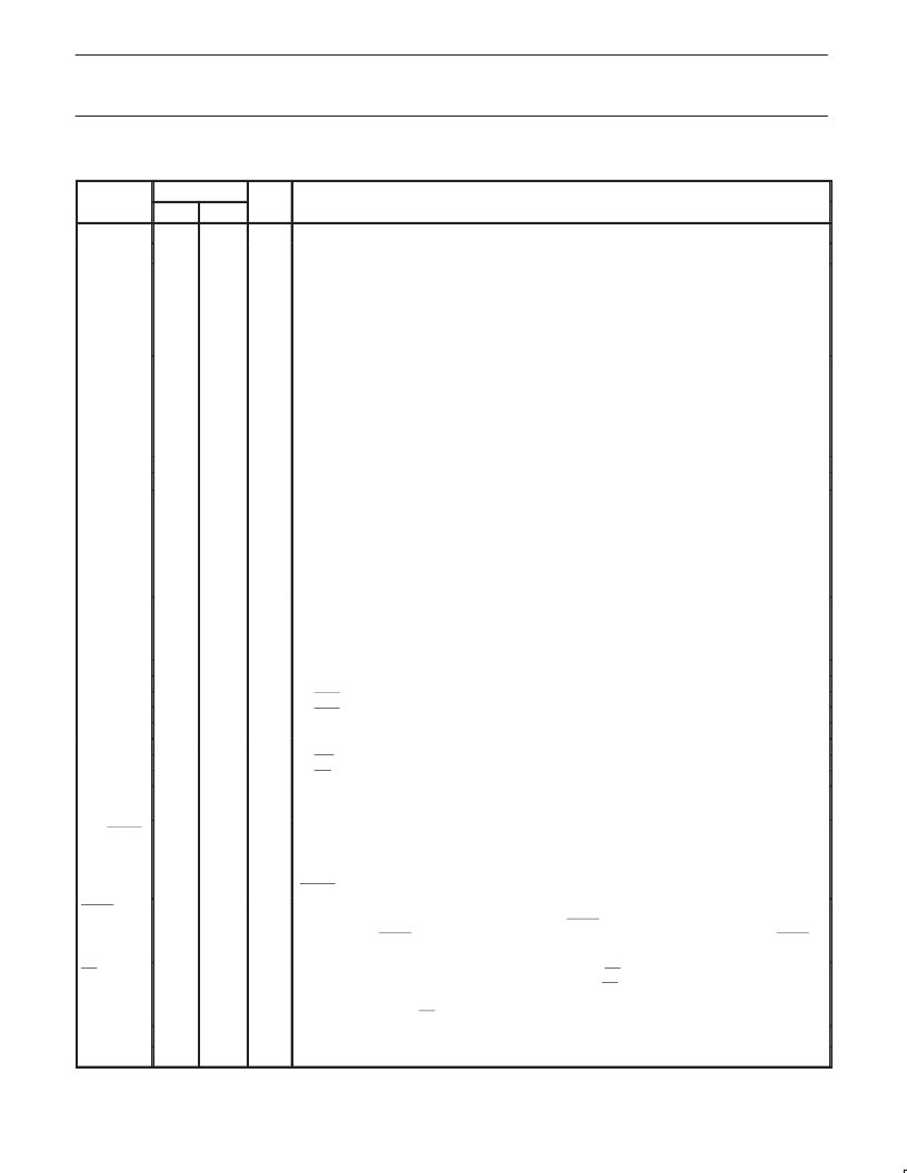
PIN DESCRIPTIONS
PIN NUMBER
MNEMONIC
LCC
QFP
TYPE
NAME AND FUNCTION
V
SS
V
CC
P0.0–0.7
1, 22
16, 39
I
Ground:
0V reference.
23, 44
17, 38
I
Power Supply:
This is the power supply voltage for normal, idle, and power-down operation.
43–36
37–30
I/O
Port 0:
Port 0 is an open-drain, bidirectional I/O port. Port 0 pins that have 1s written to them float
and can be used as high-impedance inputs. Port 0 is also the multiplexed low-order address and
data bus during accesses to external program and data memory. In this application, it uses strong
internal pull-ups when emitting 1s. Port 0 also outputs the code bytes during program verification and
received code bytes during EEPROM programming. External pull-ups are required during program
verification.
P1.0–P1.7
2–9
40–44,
1–3
I/O
Port 1:
Port 1 is an 8-bit bidirectional I/O port with internal pull-ups. Port 1 pins that have 1s written
to them are pulled high by the internal pull-ups and can be used as inputs. As inputs, port 1 pins that
are externally pulled low will source current because of the internal pull-ups. (See DC Electrical
Characteristics: I
IL
). Port 1 also receives the low-order address byte during program memory
verification.
Alternate functions for Port 1 include:
T2 (P1.0):
Timer/Counter 2 external count input
T2EX (P1.1):
Timer/Counter 2 Reload/Capture
2
3
40
41
I/O
I
P2.0–P2.7
24–31
18–25
I/O
Port 2:
Port 2 is an 8-bit bidirectional I/O port with internal pull-ups. Port 2 pins that have 1s written
to them are pulled high by the internal pull-ups and can be used as inputs. As inputs, port 2 pins that
are externally being pulled low will source current because of the internal pull-ups. (See DC
Electrical Characteristics: I
IL
). Port 2 emits the high-order address byte during fetches from external
program memory and during accesses to external data memory that use 16-bit addresses (MOVX
@DPTR). In this application, it uses strong internal pull-ups when emitting 1s. Some Port 2 pins
receive the high order address bits during EEPROM programming and verification.
P3.0–P3.7
11,
13–19
5,
7–13
I/O
Port 3:
Port 3 is an 8-bit bidirectional I/O port with internal pull-ups. Port 3 pins that have 1s written
to them are pulled high by the internal pull-ups and can be used as inputs. As inputs, port 3 pins that
are externally being pulled low will source current because of the pull-ups. (See DC Electrical
Characteristics: I
IL
). Port 3 also serves the special features of the 80C51 family, as listed below:
RxD (P3.0):
Serial input port
TxD (P3.1):
Serial output port
INT0 (P3.2):
External interrupt
INT1 (P3.3):
External interrupt
T0 (P3.4):
Timer 0 external input
T1 (P3.5):
Timer 1 external input
WR (P3.6):
External data memory write strobe
RD (P3.7):
External data memory read strobe
11
13
14
15
16
17
18
19
5
7
8
9
10
11
12
13
I
O
I
I
I
I
O
O
RST
10
4
I
Reset:
A high on this pin for two machine cycles while the oscillator is running, resets the device. An
internal diffused resistor to V
SS
permits a power-on reset using only an external capacitor to V
CC
.
Address Latch Enable/Program Pulse:
Output pulse for latching the low byte of the address
during an access to external memory. In normal operation, ALE is emitted at a constant rate of 1/6
the oscillator frequency, and can be used for external timing or clocking. Note that one ALE pulse is
skipped during each access to external data memory. This pin is also the program pulse input
(PROG) during EEPROM programming.
ALE/PROG
33
27
O
PSEN
32
26
O
Program Store Enable:
The read strobe to external program memory. When the processor is
executing code from the external program memory, PSEN is activated twice each machine cycle,
except that two PSEN activations are skipped during each access to external data memory. PSEN is
not activated during fetches from internal program memory.
EA/V
PP
35
29
I
External Access Enable/Programming Supply Voltage:
EA must be externally held low to enable
the device to fetch code from external program memory. If EA is held high, the device executes from
internal program memory. This pin also receives the 12V programming supply voltage (V
PP
) during
EPROM programming. EA is internally latched on Reset.
XTAL1
21
15
I
Crystal 1:
Input to the inverting oscillator amplifier and input to the internal clock generator circuits.
XTAL2
20
14
O
Crystal 2:
Output from the inverting oscillator amplifier.
NOTE:
To avoid “latch-up” effect at power-on, the voltage on any pin at any time must not be higher than V
CC
+ 0.5V or V
SS
– 0.5V, respectively.
相关PDF资料 |
PDF描述 |
|---|---|
| P89C536NBBB | CMOS single-chip 8-bit microcontrollers with FLASH program memory |
| P89C538NBBB | CMOS single-chip 8-bit microcontrollers with FLASH program memory |
| P89C535NBAA | CMOS single-chip 8-bit microcontrollers with FLASH program memory |
| P89C538NBAA | CMOS single-chip 8-bit microcontrollers with FLASH program memory |
| P89C557E4 | Single-chip 8-bit microcontroller(单片8位微控制器) |
相关代理商/技术参数 |
参数描述 |
|---|---|
| P89C536NBBB | 制造商:PHILIPS 制造商全称:NXP Semiconductors 功能描述:80C51 8-bit microcontroller family 16K/64K/512 FLASH |
| P89C538NBAA | 制造商:PHILIPS 制造商全称:NXP Semiconductors 功能描述:80C51 8-bit microcontroller family 16K/64K/512 FLASH |
| P89C538NBBB | 制造商:PHILIPS 制造商全称:NXP Semiconductors 功能描述:80C51 8-bit microcontroller family 16K/64K/512 FLASH |
| P89C54BA | 制造商:PHILIPS 制造商全称:NXP Semiconductors 功能描述:80C51 8-bit microcontroller family 4K/8K/16K/32K Flash |
| P89C54BBD | 制造商:未知厂家 制造商全称:未知厂家 功能描述:MICROCONTROLLER|8-BIT|8051 CPU|CMOS|QFP|44PIN|PLASTIC |
发布紧急采购,3分钟左右您将得到回复。