- 您现在的位置:买卖IC网 > PDF目录367742 > P89C668HBBD (NXP SEMICONDUCTORS) 80C51 8-bit Flash microcontroller family 64KB ISP FLASH with 8KB RAM PDF资料下载
参数资料
| 型号: | P89C668HBBD |
| 厂商: | NXP SEMICONDUCTORS |
| 元件分类: | 微控制器/微处理器 |
| 英文描述: | 80C51 8-bit Flash microcontroller family 64KB ISP FLASH with 8KB RAM |
| 中文描述: | 8-BIT, FLASH, 33 MHz, MICROCONTROLLER, PQFP44 |
| 封装: | 10 X 10 MM, 1.40 MM HEIGHT, PLASTIC, MS-026, SOT-389-1, LQFP-44 |
| 文件页数: | 5/54页 |
| 文件大小: | 299K |
| 代理商: | P89C668HBBD |
第1页第2页第3页第4页当前第5页第6页第7页第8页第9页第10页第11页第12页第13页第14页第15页第16页第17页第18页第19页第20页第21页第22页第23页第24页第25页第26页第27页第28页第29页第30页第31页第32页第33页第34页第35页第36页第37页第38页第39页第40页第41页第42页第43页第44页第45页第46页第47页第48页第49页第50页第51页第52页第53页第54页
Philips Semiconductors
Preliminary data
P89C668
80C51 8-bit Flash microcontroller family
64KB ISP Flash with 8KB RAM
2001 Jul 27
5
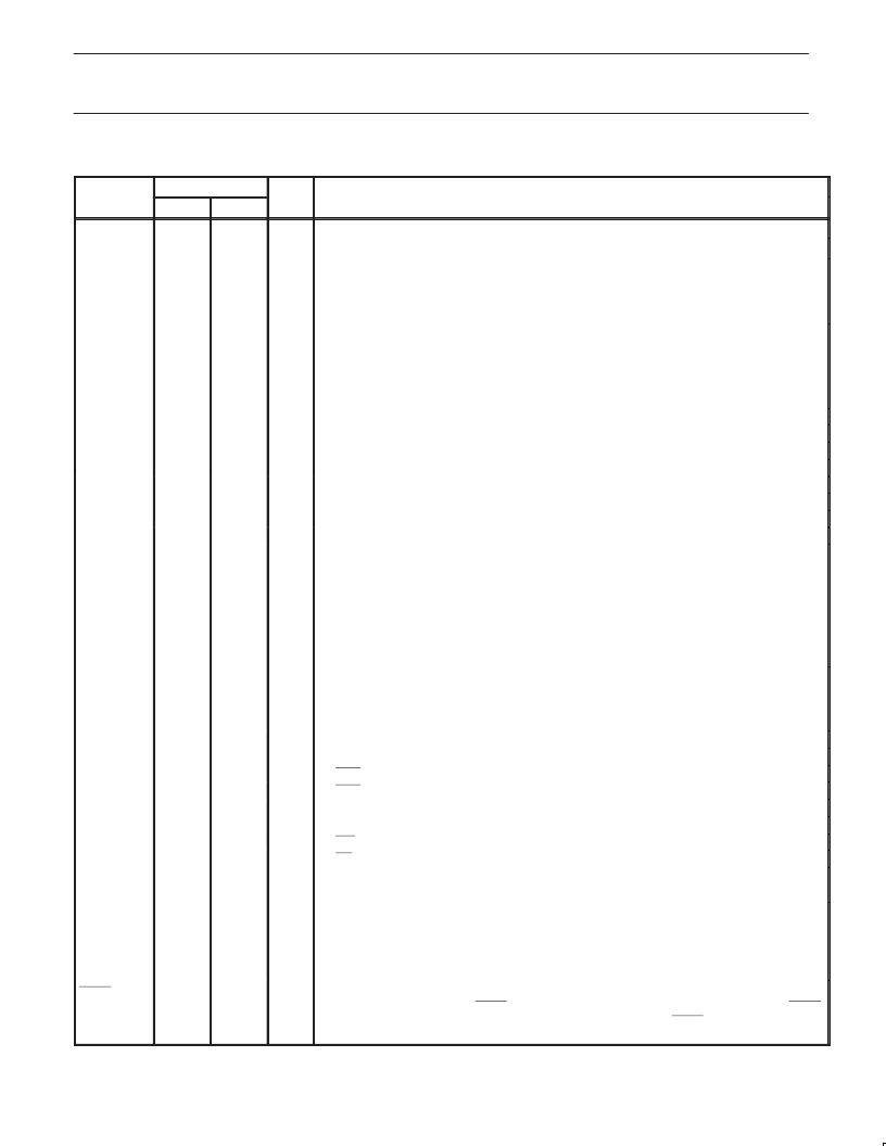
PIN DESCRIPTIONS
MNEMONIC
PIN NUMBER
NAME AND FUNCTION
PLCC
LQFP
V
SS
V
CC
P0.0–0.7
22
16
I
Ground:
0 V reference.
44
38
I
Power Supply:
This is the power supply voltage for normal, idle, and power-down operation.
43–36
37–30
I/O
Port 0:
Port 0 is an open-drain, bidirectional I/O port. Port 0 pins that have 1s written to them float
and can be used as high-impedance inputs. Port 0 is also the multiplexed low-order address and
data bus during accesses to external program and data memory. In this application, it uses strong
internal pull-ups when emitting 1s.
P1.0–P1.7
2–9
40–44,
1–3
I/O
Port 1:
Port 1 is an 8-bit bidirectional I/O port with internal pull-ups on all pins except P1.6 and
P1.7 which are open drain. Port 1 pins that have 1s written to them are pulled high by the internal
pull-ups and can be used as inputs. As inputs, port 1 pins that are externally pulled low will source
current because of the internal pull-ups. (See DC Electrical Characteristics: I
IL
).
Alternate functions for P89C668 Port 1 include:
T2 (P1.0):
Timer/Counter 2 external count input/Clockout (see Programmable Clock-Out)
T2EX (P1.1):
Timer/Counter 2 Reload/Capture/Direction Control
ECI (P1.2):
External Clock Input to the PCA
CEX0 (P1.3):
Capture/Compare External I/O for PCA module 0
CEX1 (P1.4):
Capture/Compare External I/O for PCA module 1
CEX2 (P1.5):
Capture/Compare External I/O for PCA module 2
SCL (P1.6):
I
2
C bus clock line (open drain)
SDA (P1.7):
I
2
C bus data line (open drain)
2
3
4
5
6
7
8
9
40
41
42
43
44
1
2
3
I/O
I
I
I/O
I/O
I/O
I/O
I/O
P2.0–P2.7
24–31
18–25
I/O
Port 2:
Port 2 is an 8-bit bidirectional I/O port with internal pull-ups. Port 2 pins that have 1s
written to them are pulled high by the internal pull-ups and can be used as inputs. As inputs, port 2
pins that are externally being pulled low will source current because of the internal pull-ups. (See
DC Electrical Characteristics: I
IL
). Port 2 emits the high-order address byte during fetches from
external program memory and during accesses to external data memory that use 16-bit addresses
(MOVX @DPTR). In this application, it uses strong internal pull-ups when emitting 1s. During
accesses to external data memory that use 8-bit addresses (MOV @Ri), port 2 emits the contents
of the P2 special function register.
P3.0–P3.7
11,
13–19
5, 7–13
I/O
Port 3:
Port 3 is an 8-bit bidirectional I/O port with internal pull-ups. Port 3 pins that have 1s written
to them are pulled high by the internal pull-ups and can be used as inputs. As inputs, port 3 pins that
are externally being pulled low will source current because of the pull-ups. (See DC Electrical
Characteristics: I
IL
). Port 3 also serves the special features of the P89C668, as listed below:
RxD (P3.0):
Serial input port
TxD (P3.1):
Serial output port
INT0 (P3.2):
External interrupt
INT1 (P3.3):
External interrupt
CEX3/T0 (P3.4):
Timer 0 external input; Capture/Compare External I/O for PCA module 3
CEX4/T1 (P3.5):
Timer 1 external input; Capture/Compare External I/O for PCA module 4
WR (P3.6):
External data memory write strobe
RD (P3.7):
External data memory read strobe
11
13
14
15
16
17
18
19
5
7
8
9
10
11
12
13
I
O
I
I
I
I
O
O
RST
10
4
I
Reset:
A high on this pin for two machine cycles while the oscillator is running, resets the device. An
internal diffused resistor to V
SS
permits a power-on reset using only an external capacitor to V
CC
.
Address Latch Enable:
Output pulse for latching the low byte of the address during an access to
external memory. In normal operation, ALE is emitted at a constant rate of 1/6 the oscillator
frequency, and can be used for external timing or clocking. Note that one ALE pulse is skipped
during each access to external data memory. ALE can be disabled by setting SFR auxiliary.0.
With this bit set, ALE will be active only during a MOVX instruction.
ALE
33
27
O
PSEN
32
26
O
Program Store Enable:
The read strobe to external program memory. When executing code from
the external program memory, PSEN is activated twice each machine cycle, except that two PSEN
activations are skipped during each access to external data memory. PSEN is not activated during
fetches from internal program memory.
相关PDF资料 |
PDF描述 |
|---|---|
| P89CE558 | Single-chip 8-bit microcontroller(8位单片微控制器) |
| P83CE558 | Single-chip 8-bit microcontroller |
| P89CE558EBB | Single-chip 8-bit microcontroller |
| P89CE558EFB | Single-chip 8-bit microcontroller |
| P80CE558 | Single-chip 8-bit microcontroller(8位单片微控制器) |
相关代理商/技术参数 |
参数描述 |
|---|---|
| P89C668HBBD/00,557 | 功能描述:8位微控制器 -MCU 64K/8K FL 6CLK ISP/IAP QFP COM RoHS:否 制造商:Silicon Labs 核心:8051 处理器系列:C8051F39x 数据总线宽度:8 bit 最大时钟频率:50 MHz 程序存储器大小:16 KB 数据 RAM 大小:1 KB 片上 ADC:Yes 工作电源电压:1.8 V to 3.6 V 工作温度范围:- 40 C to + 105 C 封装 / 箱体:QFN-20 安装风格:SMD/SMT |
| P89C668HFA | 功能描述:8位微控制器 -MCU 80C51 64K FL / 8K RM RoHS:否 制造商:Silicon Labs 核心:8051 处理器系列:C8051F39x 数据总线宽度:8 bit 最大时钟频率:50 MHz 程序存储器大小:16 KB 数据 RAM 大小:1 KB 片上 ADC:Yes 工作电源电压:1.8 V to 3.6 V 工作温度范围:- 40 C to + 105 C 封装 / 箱体:QFN-20 安装风格:SMD/SMT |
| P89C668HFA/00,512 | 功能描述:8位微控制器 -MCU 64K/8K FL 6CLK ISP/IAP PLCC IN RoHS:否 制造商:Silicon Labs 核心:8051 处理器系列:C8051F39x 数据总线宽度:8 bit 最大时钟频率:50 MHz 程序存储器大小:16 KB 数据 RAM 大小:1 KB 片上 ADC:Yes 工作电源电压:1.8 V to 3.6 V 工作温度范围:- 40 C to + 105 C 封装 / 箱体:QFN-20 安装风格:SMD/SMT |
| P89C669 | 制造商:PHILIPS 制造商全称:NXP Semiconductors 功能描述:80C51 8-bit microcontroller family with extended memory 96 kB Flash with 2 kB RAM |
| P89C669BBD | 制造商:PHILIPS 制造商全称:NXP Semiconductors 功能描述:80C51 8-bit microcontroller family with extended memory 96 kB Flash with 2 kB RAM |
发布紧急采购,3分钟左右您将得到回复。