- 您现在的位置:买卖IC网 > PDF目录1959 > P89LPC9351FA,112 (NXP Semiconductors)IC 80C51 MCU FLASH 8K 28-PLCC PDF资料下载
参数资料
| 型号: | P89LPC9351FA,112 |
| 厂商: | NXP Semiconductors |
| 文件页数: | 26/94页 |
| 文件大小: | 0K |
| 描述: | IC 80C51 MCU FLASH 8K 28-PLCC |
| 产品培训模块: | LPC9351/9321 Overview |
| 标准包装: | 2,368 |
| 系列: | LPC900 |
| 核心处理器: | 8051 |
| 芯体尺寸: | 8-位 |
| 速度: | 18MHz |
| 连通性: | I²C,SPI,UART/USART |
| 外围设备: | 欠压检测/复位,POR,PWM,温度传感器,WDT |
| 输入/输出数: | 26 |
| 程序存储器容量: | 8KB(8K x 8) |
| 程序存储器类型: | 闪存 |
| EEPROM 大小: | 512 x 8 |
| RAM 容量: | 768 x 8 |
| 电压 - 电源 (Vcc/Vdd): | 2.4 V ~ 3.6 V |
| 数据转换器: | A/D 8x8b; D/A 2x8b |
| 振荡器型: | 内部 |
| 工作温度: | -40°C ~ 85°C |
| 封装/外壳: | 28-PLCC |
| 包装: | 管件 |
| 产品目录页面: | 706 (CN2011-ZH PDF) |
| 配用: | 622-1014-ND - BOARD FOR LPC9XX TSSOP 622-1006-ND - SOCKET ADAPTER BOARD 568-4000-ND - DEMO BOARD SPI/I2C TO DUAL UART 568-3510-ND - DEMO BOARD SPI/I2C TO UART 568-1759-ND - EMULATOR DEBUGGER/PROGRMMR LPC9X 568-1758-ND - BOARD EVAL FOR LPC93X MCU FAMILY |
| 其它名称: | 568-4701-5 935287627112 P89LPC9351FA |
第1页第2页第3页第4页第5页第6页第7页第8页第9页第10页第11页第12页第13页第14页第15页第16页第17页第18页第19页第20页第21页第22页第23页第24页第25页当前第26页第27页第28页第29页第30页第31页第32页第33页第34页第35页第36页第37页第38页第39页第40页第41页第42页第43页第44页第45页第46页第47页第48页第49页第50页第51页第52页第53页第54页第55页第56页第57页第58页第59页第60页第61页第62页第63页第64页第65页第66页第67页第68页第69页第70页第71页第72页第73页第74页第75页第76页第77页第78页第79页第80页第81页第82页第83页第84页第85页第86页第87页第88页第89页第90页第91页第92页第93页第94页
P89LPC9331_9341_9351_9361
All information provided in this document is subject to legal disclaimers.
NXP B.V. 2012. All rights reserved.
Product data sheet
Rev. 5.1 — 20 August 2012
32 of 94
NXP Semiconductors
P89LPC9331/9341/9351/9361
8-bit microcontroller with accelerated two-clock 80C51 core
7.10 CCLK wake-up delay
The P89LPC9331/9341/9351/9361 has an internal wake-up timer that delays the clock
until it stabilizes depending on the clock source used. If the clock source is any of the
three crystal selections (low, medium and high frequencies) the delay is 1024 OSCCLK
cycles plus 60
sto100 s. If the clock source is the internal RC oscillator, the delay is
200
s to 300 s. If the clock source is watchdog oscillator or external clock, the delay is
32 OSCCLK cycles.
7.11 CCLK modification: DIVM register
The OSCCLK frequency can be divided down up to 510 times by configuring a dividing
register, DIVM, to generate CCLK. This feature makes it possible to temporarily run the
CPU at a lower rate, reducing power consumption. By dividing the clock, the CPU can
retain the ability to respond to events that would not exit Idle mode by executing its normal
program at a lower rate. This can also allow bypassing the oscillator start-up time in cases
where Power-down mode would otherwise be used. The value of DIVM may be changed
by the program at any time without interrupting code execution.
7.12 Low power select
The P89LPC9331/9341/9351/9361 is designed to run at 18 MHz (CCLK) maximum.
However, if CCLK is 8 MHz or slower, the CLKLP SFR bit (AUXR1.7) can be set to logic 1
to lower the power consumption further. On any reset, CLKLP is logic 0 allowing highest
performance access. This bit can then be set in software if CCLK is running at 8 MHz or
slower.
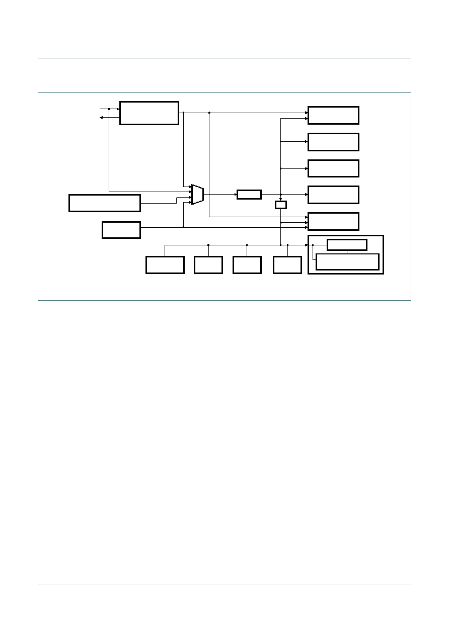
Fig 7.
Block diagram of oscillator control
÷2
002aad559
RTC
ADC1
ADC0
CPU
WDT
DIVM
CCLK
UART
OSCCLK
I2C-BUS
PCLK
TIMER 0 AND
TIMER 1
HIGH FREQUENCY
MEDIUM FREQUENCY
LOW FREQUENCY
XTAL1
XTAL2
RC OSCILLATOR
WITH CLOCK DOUBLER
WATCHDOG
OSCILLATOR
(7.3728 MHz/14.7456 MHz
± 1 %)
PCLK
RCCLK
SPI
CCU
(P89LPC9351/9361)
32
× PLL
(400 kHz
± 5 %)
相关PDF资料 |
PDF描述 |
|---|---|
| P89LPC936FDH,518 | IC 80C51 MCU FLASH 16K 28TSSOP |
| P89LPC938FDH,529 | IC 80C51 MCU FLASH 8K 28-TSSOP |
| P89LPC9401FBD,557 | IC 80C51 MCU FLASH 8K 64-LQFP |
| P89LPC9402FBD,557 | IC 80C51 MCU FLASH 8K 64-LQFP |
| P89LPC954FBD44,151 | IC 80C51 MCU FLASH 16K 44LQFP |
相关代理商/技术参数 |
参数描述 |
|---|---|
| P89LPC9351FDH | 制造商:PHILIPS 制造商全称:NXP Semiconductors 功能描述:8-bit microcontroller with accelerated two-clock 80C51 core 8 kB 3 V byte-erasable flash with 8-bit ADC |
| P89LPC9351FDH,518 | 功能描述:8位微控制器 -MCU Enhanced LPC935 RoHS:否 制造商:Silicon Labs 核心:8051 处理器系列:C8051F39x 数据总线宽度:8 bit 最大时钟频率:50 MHz 程序存储器大小:16 KB 数据 RAM 大小:1 KB 片上 ADC:Yes 工作电源电压:1.8 V to 3.6 V 工作温度范围:- 40 C to + 105 C 封装 / 箱体:QFN-20 安装风格:SMD/SMT |
| P89LPC935FA | 制造商:NXP Semiconductors 功能描述:IC MCU 8BIT 80C51 8K FLASH PLCC28 |
| P89LPC935FA,129 | 功能描述:8位微控制器 -MCU 80C51 8K FL 768B RAM RoHS:否 制造商:Silicon Labs 核心:8051 处理器系列:C8051F39x 数据总线宽度:8 bit 最大时钟频率:50 MHz 程序存储器大小:16 KB 数据 RAM 大小:1 KB 片上 ADC:Yes 工作电源电压:1.8 V to 3.6 V 工作温度范围:- 40 C to + 105 C 封装 / 箱体:QFN-20 安装风格:SMD/SMT |
| P89LPC935FA129 | 制造商:NXP Semiconductors 功能描述:IC 8BIT MCU 80C51 18MHZ LCC-28 |
发布紧急采购,3分钟左右您将得到回复。