- 您现在的位置:买卖IC网 > PDF目录367750 > PA28F200CV-T60 (Intel Corp.) 2-MBIT SmartVoltage BOOT BLOCK FLASH MEMORY FAMILY PDF资料下载
参数资料
| 型号: | PA28F200CV-T60 |
| 厂商: | Intel Corp. |
| 英文描述: | 2-MBIT SmartVoltage BOOT BLOCK FLASH MEMORY FAMILY |
| 中文描述: | 2兆位SmartVoltage启动块闪存系列 |
| 文件页数: | 15/48页 |
| 文件大小: | 562K |
| 代理商: | PA28F200CV-T60 |
第1页第2页第3页第4页第5页第6页第7页第8页第9页第10页第11页第12页第13页第14页当前第15页第16页第17页第18页第19页第20页第21页第22页第23页第24页第25页第26页第27页第28页第29页第30页第31页第32页第33页第34页第35页第36页第37页第38页第39页第40页第41页第42页第43页第44页第45页第46页第47页第48页
28F200BX-T/B, 28F002BX-T/B
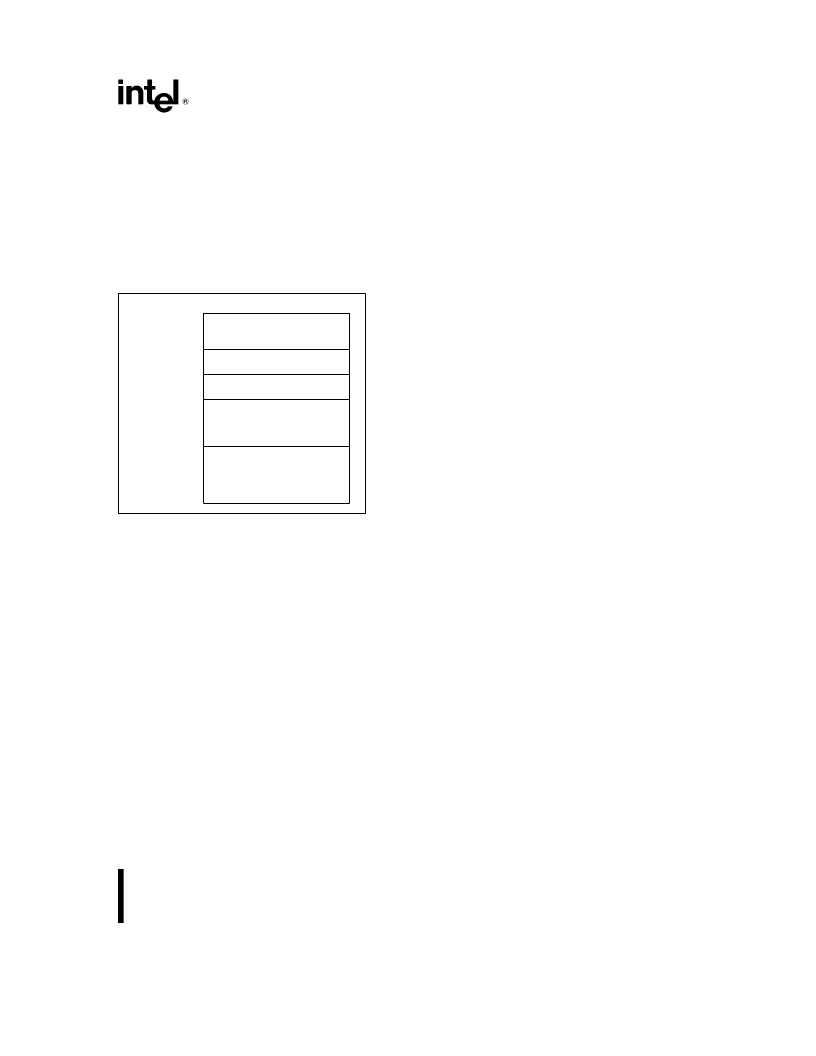
3.1.2.2 28F002BX-T Memory Map
The 28F002BX-T device has the 16-Kbyte boot
block located from 3C000H to 3FFFFH to accom-
modate those microprocessors that boot from the
top of the address map. In the 28F002BX-T the first
8-Kbyte parmeter block resides in memory space
from 3A000H to 3BFFFH. The second 8-Kbyte pa-
rameter block resides in memory space from
38000H to 39FFFH. The 96-Kbyte main block re-
sides in memory space from 20000H to 37FFFH.
The 128-Kbyte main block resides in memory space
from 00000H to 1FFFFH.
3FFFFH
16-Kbyte BOOT BLOCK
3BFFFH
3C000H
8-Kbyte PARAMETER BLOCK
39FFFH
3A000H
8-Kbyte PARAMETER BLOCK
37FFFH
38000H
96-Kbyte MAIN BLOCK
1FFFFH
20000H
128-Kbyte MAIN BLOCK
00000H
Figure 11. 28F002BX-T Memory Map
4.0 PRODUCT FAMILY PRINCIPLES
OF OPERATION
Flash memory augments EPROM functionality with
in-circuit electrical write and erase. The 2-Mbit flash
family utilizes a Command User Interface (CUI) and
internally generated and timed algorithms to simplify
write and erase operations.
The CUI allows for 100% TTL-level control inputs,
fixed power supplies during erasure and program-
ming, and maximum EPROM compatibility.
In the absence of high voltage on the V
PP
pin, the
2-Mbit boot block flash family will only successfully
execute the following commands: Read Array, Read
Status Register, Clear Status Register and Intelli-
gent Identifier mode. The device provides standard
EPROM read, standby and output disable opera-
tions. Manufacturer Identification and Device Identi-
fication data can be accessed through the CUI or
through the standard EPROM A9 high voltage ac-
cess (V
ID
) for PROM programming equipment.
The same EPROM read, standby and output disable
functions are available when high voltage is applied
to the V
PP
pin. In addition, high voltage on V
PP
al-
lows write and erase of the device. All functions as-
sociated with altering memory contents: write and
erase, Intelligent Identifier read and Read Status are
accessed via the CUI.
The purpose of the Write State Machine (WSM) is to
completely automate the write and erasure of the
device. The WSM will begin operation upon receipt
of a signal from the CUI and will report status back
through a Status Register. The CUI will handle the
WE
Y
interface to the data and address latches, as
well as system software requests for status while the
WSM is in operation.
4.1 28F200BX Bus Operations
Flash memory reads, erases and writes in-system
via the local CPU. All bus cycles to or from the flash
memory conform to standard microprocessor bus
cycles.
15
相关PDF资料 |
PDF描述 |
|---|---|
| PA28F200CV-T80 | 2-MBIT SmartVoltage BOOT BLOCK FLASH MEMORY FAMILY |
| PA28F200BL-T150 | 2-MBIT (128K x 16, 256K x 8)LOW-POWER BOOT BLOCK FLASH MEMORY FAMILY |
| PA28F200BV-T80 | POWERLINE: RP40-S_D_TE - 2:1 Wide Input Voltage Range- 40 Watts Output Power- 1.6kVDC Isolation- Fixed Operating Frequency- Six-Sided Continuous Shield- Design Meet Safety Standard- Standard 76.2 x66.0x10.2mm Package- Efficiency to 90% |
| PA28F200BV-B60 | 2-MBIT SmartVoltage BOOT BLOCK FLASH MEMORY FAMILY |
| PA28F200BV-B80 | 2-MBIT SmartVoltage BOOT BLOCK FLASH MEMORY FAMILY |
相关代理商/技术参数 |
参数描述 |
|---|---|
| PA28F200CV-T80 | 制造商:INTEL 制造商全称:Intel Corporation 功能描述:2-MBIT SmartVoltage BOOT BLOCK FLASH MEMORY FAMILY |
| PA28F400B5B60 | 制造商:Intel 功能描述: |
| PA28F400B5B80 | 制造商:INTEL 制造商全称:Intel Corporation 功能描述:SMART 5 BOOT BLOCK FLASH MEMORY FAMILY 2, 4, 8 MBIT |
| PA28F400B5T60 | 制造商:Intel 功能描述: |
| PA28F400B5T80 | 制造商:Intel 功能描述:Flash Mem Parallel 5V 4M-Bit 512K x 8/256K x 16 80ns 44-Pin SOP |
发布紧急采购,3分钟左右您将得到回复。