- 您现在的位置:买卖IC网 > PDF目录367750 > PA28F400BX-T80 (INTEL CORP) 4-MBIT (256K X 16, 512K X 8) BOOT BLOCK FLASH MEMORY FAMILY PDF资料下载
参数资料
| 型号: | PA28F400BX-T80 |
| 厂商: | INTEL CORP |
| 元件分类: | PROM |
| 英文描述: | 4-MBIT (256K X 16, 512K X 8) BOOT BLOCK FLASH MEMORY FAMILY |
| 中文描述: | 256K X 16 FLASH 12V PROM, 80 ns, PDSO40 |
| 封装: | 1.110 X 0.525 INCH, PLASTIC, SOP-40 |
| 文件页数: | 18/50页 |
| 文件大小: | 559K |
| 代理商: | PA28F400BX-T80 |
第1页第2页第3页第4页第5页第6页第7页第8页第9页第10页第11页第12页第13页第14页第15页第16页第17页当前第18页第19页第20页第21页第22页第23页第24页第25页第26页第27页第28页第29页第30页第31页第32页第33页第34页第35页第36页第37页第38页第39页第40页第41页第42页第43页第44页第45页第46页第47页第48页第49页第50页
28F400BX-T/B, 28F004BX-T/B
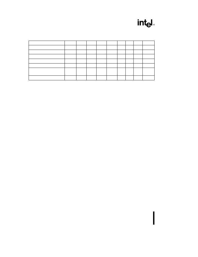
4.2 28F004BX Bus Operations
Table 3. Bus Operations
Mode
Notes
RP
Y
CE
Y
OE
Y
WE
Y
A
9
A
0
V
PP
DQ
0–7
Read
1, 2
V
IH
V
IL
V
IL
V
IH
X
X
X
D
OUT
Output Disable
V
IH
V
IL
V
IH
V
IH
X
X
X
High Z
Standby
V
IH
V
IH
X
X
X
X
X
High Z
Deep Power-Down
9
V
IL
X
X
X
X
X
X
High Z
Intelligent Identifier (Mfr)
3, 4
V
IH
V
IL
V
IL
V
IH
V
ID
V
IL
X
89H
Intelligent Identifier (Device)
3, 4, 5
V
IH
V
IL
V
IL
V
IH
V
ID
V
IH
X
78H
79H
Write
6, 7, 8
V
IH
V
IL
V
IH
V
IL
X
X
X
D
IN
NOTES:
1. Refer to DC Characteristics.
2. X can be V
IL
or V
IH
for control pins and addresses, V
PPL
or V
PPH
for V
PP
.
3. See DC Characteristics for V
PPL
, V
PPH
, V
HH
, V
ID
voltages.
4. Manufacturer and Device codes may also be accessed via a CUI write sequence. A
1
–A
18
e
X.
5. Device ID
e
78H for 28F004BX-T and 79H for 28F004BX-B.
6. Refer to Table 4 for valid D
IN
during a write operation.
7. Command writes for Block erase or byte program are only executed when V
PP
e
V
PPH
.
6. Program or erase the Boot block by holding RP
Y
at V
HH
.
9. RP
Y
must be at GND
g
0.2V to meet the 1.2
m
A maximum deep power-down current.
4.3 Read Operations
The 4-Mbit boot block flash family has three user
read modes; Array, Intelligent Identifier, and Status
Register. Status Register read mode will be dis-
cussed in detail in the ‘‘Write Operations’’ section.
During power-up conditions (V
CC
supply ramping), it
takes a maximum of 600 ns from when V
CC
is at
4.5V minimum to valid data on the outputs.
4.3.1 READ ARRAY
If the memory is not in the Read Array mode, it is
necessary to write the appropriate read mode com-
mand to the CUI. The 4-Mbit boot block flash family
has three control functions, all of which must be
logically active, to obtain data at the outputs.
Chip-Enable CE
Y
is the device selection control.
Power-Down RP
Y
is the device power control. Out-
put-Enable OE
Y
is the DATA INPUT/OUTPUT
(DQ
[
0:15
]
or DQ
[
0:7
]
) direction control and when
active is used to drive data from the selected memo-
ry on to the I/O bus.
4.3.1.1 Output Control
With OE
Y
at logic-high level (V
IH
), the output from
the device is disabled and data input/output pins
(DQ
[
0:15
]
or DQ
[
0:7
]
are tri-stated. Data input is
then controlled by WE
Y
.
4.3.1.2 Input Control
With WE
Y
at logic-high level (V
IH
), input to the de-
vice is disabled. Data Input/Output pins (DQ
[
0:15
]
or DQ
[
0:7
]
) are controlled by OE
Y
.
4.3.2 INTELLIGENT IDENTIFIERS
28F400BX PRODUCTS
The manufacturer and device codes are read via the
CUI or by taking the A
9
pin to 12V. Writing 90H to
the CUI places the device into Intelligent Identifier
read mode. A read of location 00000H outputs the
manufacturer’s identification code, 0089H, and loca-
tion 00001H outputs the device code; 4470H for
28F400BX-T,
4471H
for
BYTE
Y
is at a logic low only the lower byte of the
above signatures is read and DQ
15
/A
b
1
is a ‘‘don’t
care’’ during Intelligent Identifier mode. A read array
command must be written to the memory to return to
the read array mode.
28F400BX-B.
When
28F004BX PRODUCTS
The manufacturer and device codes are also read
via the CUI or by taking the A
9
pin to 12V. Writing
90H to the CUI places the device into Intelligent
Identifier read mode. A read of location 00000H out-
puts the manufacturer’s identification code, 89H,
and location 00001H outputs the device code; 78H
for 28F004BX-T, 79H for 28F004BX-B.
18
相关PDF资料 |
PDF描述 |
|---|---|
| PA28F400CV-B80 | 2-MBIT SmartVoltage BOOT BLOCK FLASH MEMORY FAMILY |
| PA28F400CV-T60 | 2-MBIT SmartVoltage BOOT BLOCK FLASH MEMORY FAMILY |
| PA28F400CV-T80 | 2-MBIT SmartVoltage BOOT BLOCK FLASH MEMORY FAMILY |
| PA28F400BL-T150 | ECONOLINE: RM & RL - Single Output Rail- Industry Standard Pinout- 1kVDC & 2kVDC Isolation- High Efficiency for Low Power Applications- UL94V-0 Package Material- Toroidal Magnetics- Fully Encapsulated- Efficiency to 80% |
| PA28F400BV-T60 | POWERLINE: RP40-S_D_TE - 2:1 Wide Input Voltage Range- 40 Watts Output Power- 1.6kVDC Isolation- Fixed Operating Frequency- Six-Sided Continuous Shield- Design Meet Safety Standard- Standard 76.2 x66.0x10.2mm Package- Efficiency to 90% |
相关代理商/技术参数 |
参数描述 |
|---|---|
| PA28F400CV-B60 | 制造商:INTEL 制造商全称:Intel Corporation 功能描述:2-MBIT SmartVoltage BOOT BLOCK FLASH MEMORY FAMILY |
| PA28F400CV-B80 | 制造商:INTEL 制造商全称:Intel Corporation 功能描述:2-MBIT SmartVoltage BOOT BLOCK FLASH MEMORY FAMILY |
| PA28F400CV-T60 | 制造商:INTEL 制造商全称:Intel Corporation 功能描述:2-MBIT SmartVoltage BOOT BLOCK FLASH MEMORY FAMILY |
| PA28F400CV-T80 | 制造商:INTEL 制造商全称:Intel Corporation 功能描述:2-MBIT SmartVoltage BOOT BLOCK FLASH MEMORY FAMILY |
| PA28F800B5B70 | 制造商:INTEL 制造商全称:Intel Corporation 功能描述:SMART 5 BOOT BLOCK FLASH MEMORY FAMILY 2, 4, 8 MBIT |
发布紧急采购,3分钟左右您将得到回复。