- 您现在的位置:买卖IC网 > PDF目录3778 > PCA9539BS,118 (NXP Semiconductors)IC I/O EXPANDER I2C 16B 24HVQFN PDF资料下载
参数资料
| 型号: | PCA9539BS,118 |
| 厂商: | NXP Semiconductors |
| 文件页数: | 6/37页 |
| 文件大小: | 0K |
| 描述: | IC I/O EXPANDER I2C 16B 24HVQFN |
| 产品培训模块: | I²C Bus Fundamentals |
| 特色产品: | NXP - I2C Interface |
| 标准包装: | 1 |
| 接口: | I²C,SM 总线 |
| 输入/输出数: | 16 |
| 中断输出: | 是 |
| 频率 - 时钟: | 400kHz |
| 电源电压: | 2.3 V ~ 5.5 V |
| 工作温度: | -40°C ~ 85°C |
| 安装类型: | 表面贴装 |
| 封装/外壳: | 24-VFQFN 裸露焊盘 |
| 供应商设备封装: | 24-HVQFN(4x4) |
| 包装: | 标准包装 |
| 包括: | POR |
| 产品目录页面: | 825 (CN2011-ZH PDF) |
| 其它名称: | 568-1841-6 |
第1页第2页第3页第4页第5页当前第6页第7页第8页第9页第10页第11页第12页第13页第14页第15页第16页第17页第18页第19页第20页第21页第22页第23页第24页第25页第26页第27页第28页第29页第30页第31页第32页第33页第34页第35页第36页第37页
PCA9539_PCA9539R
All information provided in this document is subject to legal disclaimers.
NXP B.V. 2013. All rights reserved.
Product data sheet
Rev. 6 — 6 February 2013
14 of 37
NXP Semiconductors
PCA9539; PCA9539R
16-bit I2C-bus and SMBus low power I/O port with interrupt and reset
6.6.3 Interrupt output
The open-drain interrupt output is activated when one of the port pins changes state and
the pin is configured as an input. The interrupt is deactivated when the input returns to its
previous state or the Input port register is read (see Figure 10). A pin configured as an
output cannot cause an interrupt. Since each 8-bit port is read independently, the interrupt
caused by Port 0 will not be cleared by a read of Port 1 or the other way around.
Remark: Changing an I/O from an output to an input may cause a false interrupt to occur
if the state of the pin does not match the contents of the Input port register.
7.
Characteristics of the I2C-bus
The I2C-bus is for 2-way, 2-line communication between different ICs or modules. The two
lines are a serial data line (SDA) and a serial clock line (SCL). Both lines must be
connected to a positive supply via a pull-up resistor when connected to the output stages
of a device. Data transfer may be initiated only when the bus is not busy.
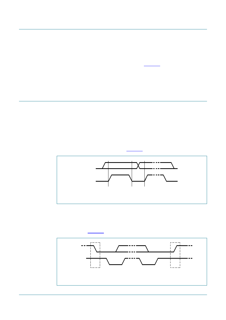
7.1 Bit transfer
One data bit is transferred during each clock pulse. The data on the SDA line must remain
stable during the HIGH period of the clock pulse as changes in the data line at this time
will be interpreted as control signals (see Figure 12).
7.1.1 START and STOP conditions
Both data and clock lines remain HIGH when the bus is not busy. A HIGH-to-LOW
transition of the data line while the clock is HIGH is defined as the START condition (S). A
LOW-to-HIGH transition of the data line while the clock is HIGH is defined as the STOP
condition (P) (see Figure 13).
Fig 12. Bit transfer
mba607
data line
stable;
data valid
change
of data
allowed
SDA
SCL
Fig 13. Definition of START and STOP conditions
mba608
SDA
SCL
P
STOP condition
S
START condition
相关PDF资料 |
PDF描述 |
|---|---|
| PCA9555PW,118 | IC I/O EXPANDER I2C 16B 24TSSOP |
| 583859-7 | CONN CARDEDGE HSNG 15POS DL .156 |
| PCA9575HF,118 | IC I/O EXPANDER I2C 16B 24HWQFN |
| PCA9501BS,118 | IC I/O EXPANDER I2C 8B 20HVQFN |
| PCA9535BS,118 | IC I/O EXPANDER I2C 16B 24HVQFN |
相关代理商/技术参数 |
参数描述 |
|---|---|
| PCA9539BSHP | 功能描述:I/O Expander 16 I2C 400kHz 24-HVQFN (4x4) 制造商:nxp semiconductors 系列:- 包装:剪切带(CT) 零件状态:停产 I/O 数:16 接口:I2C 中断输出:是 特性:POR 输出类型:开路漏极 电流 - 灌/拉输出:50mA 频率 - 时钟:400kHz 电压 - 电源:2.3 V ~ 5.5 V 工作温度:-40°C ~ 85°C 安装类型:表面贴装 封装/外壳:24-VFQFN 裸露焊盘 供应商器件封装:24-HVQFN(4x4) 标准包装:1 |
| PCA9539BS-T | 制造商:NXP Semiconductors 功能描述:I2C/SMBus GPIO Expander 5.5V 24-Pin HVQFN EP T/R |
| PCA9539D | 功能描述:接口-I/O扩展器 I2C/SMBUS 16BIT GPIO RoHS:否 制造商:NXP Semiconductors 逻辑系列: 输入/输出端数量: 最大工作频率:100 kHz 工作电源电压:1.65 V to 5.5 V 工作温度范围:- 40 C to + 85 C 安装风格:SMD/SMT 封装 / 箱体:HVQFN-16 封装:Reel |
| PCA9539D,112 | 功能描述:接口-I/O扩展器 I2C/SMBUS 16BIT GPIO RoHS:否 制造商:NXP Semiconductors 逻辑系列: 输入/输出端数量: 最大工作频率:100 kHz 工作电源电压:1.65 V to 5.5 V 工作温度范围:- 40 C to + 85 C 安装风格:SMD/SMT 封装 / 箱体:HVQFN-16 封装:Reel |
| PCA9539D,118 | 功能描述:接口-I/O扩展器 16-BIT I2C FM TP GPIO INT RST RoHS:否 制造商:NXP Semiconductors 逻辑系列: 输入/输出端数量: 最大工作频率:100 kHz 工作电源电压:1.65 V to 5.5 V 工作温度范围:- 40 C to + 85 C 安装风格:SMD/SMT 封装 / 箱体:HVQFN-16 封装:Reel |
发布紧急采购,3分钟左右您将得到回复。