参数资料
| 型号: | PCA9670PW,112 |
| 厂商: | NXP Semiconductors |
| 文件页数: | 5/35页 |
| 文件大小: | 0K |
| 描述: | IC I/O EXPANDER I2C 8B 16TSSOP |
| 产品培训模块: | LED Controllers I²C Bus Fundamentals |
| 特色产品: | NXP - I2C Interface |
| 标准包装: | 96 |
| 接口: | I²C |
| 输入/输出数: | 8 |
| 中断输出: | 无 |
| 频率 - 时钟: | 1MHz |
| 电源电压: | 2.3 V ~ 5.5 V |
| 工作温度: | -40°C ~ 85°C |
| 安装类型: | 表面贴装 |
| 封装/外壳: | 16-TSSOP(0.173",4.40mm 宽) |
| 供应商设备封装: | 16-TSSOP |
| 包装: | 管件 |
| 包括: | POR |
| 产品目录页面: | 826 (CN2011-ZH PDF) |
| 其它名称: | 568-4189-5 935282716112 PCA9670PW |
第1页第2页第3页第4页当前第5页第6页第7页第8页第9页第10页第11页第12页第13页第14页第15页第16页第17页第18页第19页第20页第21页第22页第23页第24页第25页第26页第27页第28页第29页第30页第31页第32页第33页第34页第35页
PCA9670
All information provided in this document is subject to legal disclaimers.
NXP B.V. 2013. All rights reserved.
Product data sheet
Rev. 3 — 30 May 2013
13 of 35
NXP Semiconductors
PCA9670
Remote 8-bit I/O expander for Fm+ I2C-bus with reset
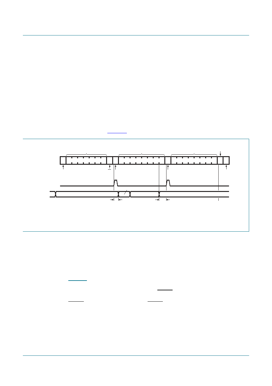
8.3 Reading from a port (Input mode)
The port must have been previously written to logic 1, which is the condition after
power-on reset or hardware reset or software reset. To enter the Read mode the master
(microcontroller) addresses the slave device and sets the last bit of the address byte to
logic 1 (address byte read). The slave will acknowledge and then send the data byte to
the master. The master will NACK and then send the STOP condition or ACK and read the
input register again.
The read of any pin being used as an output will indicate HIGH or LOW depending on the
actual state of the input pin.
If the data on the input port changes faster than the master can read, this data may be
lost. The DATA 2 and DATA 3 are lost because these data did not meet the set-up time
and hold time (see Figure 14).
8.4 Power-on reset
When power is applied to VDD, an internal Power-On Reset (POR) holds the PCA9670 in
a reset condition until VDD has reached VPOR. At that point, the reset condition is released
and the PCA9670 registers and I2C-bus/SMBus state machine will initialize to their default
states of all I/Os to inputs with weak current source to VDD. Thereafter VDD must be
lowered below VPOR and back up to the operation voltage for power-on reset cycle.
8.5 RESET input
A reset can be accomplished by holding the RESET pin LOW for a minimum of tw(rst). The
PCA9670 registers and I2C-bus state machine will be held in their default state until the
RESET input is once again HIGH. This RESET input pin requires a pull-up resistor to VDD
if no active connection is used.
A LOW-to-HIGH transition of SDA while SCL is HIGH is defined as the STOP condition (P). Transfer of data can be stopped at
any moment by a STOP condition. When this occurs, data present at the last acknowledge phase is valid (Output mode). Input
data is lost.
Fig 14. Read input port register
A5 A4 A3 A2 A1 A0
1
A
SA6
slave address
START condition
R/W
acknowledge
from slave
002aac266
data from port
A
acknowledge
from master
SDA
1
no acknowledge
from master
read from port
data at port
data from port
DATA 1
DATA 4
DATA 2
DATA 3
P
STOP
condition
th(D)
tsu(D)
DATA 1
相关PDF资料 |
PDF描述 |
|---|---|
| PCA9574BS,118 | IC I/O EXPANDER I2C 8B 16HVQFN |
| ATTINY24A-MUR | MCU AVR 2KB FLASH 20MHZ 20QFN |
| PCA8574PW,118 | IC I/O EXPANDER I2C 8B 16TSSOP |
| ATTINY24A-CCUR | MCU AVR 2KB FLASH 20MHZ 15UFBGA |
| ATTINY24A-SSNR | MCU AVR 2KB FLASH 20MHZ 14SOIC |
相关代理商/技术参数 |
参数描述 |
|---|---|
| PCA9670PW-T | 功能描述:接口-I/O扩展器 8-BIT I2C FM+ QB GPIO INT PU RoHS:否 制造商:NXP Semiconductors 逻辑系列: 输入/输出端数量: 最大工作频率:100 kHz 工作电源电压:1.65 V to 5.5 V 工作温度范围:- 40 C to + 85 C 安装风格:SMD/SMT 封装 / 箱体:HVQFN-16 封装:Reel |
| PCA9671BQ,118 | 功能描述:接口-I/O扩展器 REMOTE 16BIT GPIO RoHS:否 制造商:NXP Semiconductors 逻辑系列: 输入/输出端数量: 最大工作频率:100 kHz 工作电源电压:1.65 V to 5.5 V 工作温度范围:- 40 C to + 85 C 安装风格:SMD/SMT 封装 / 箱体:HVQFN-16 封装:Reel |
| PCA9671BQ-T | 功能描述:接口-I/O扩展器 REMOTE 16BIT GPIO FM+I2C-RESET RoHS:否 制造商:NXP Semiconductors 逻辑系列: 输入/输出端数量: 最大工作频率:100 kHz 工作电源电压:1.65 V to 5.5 V 工作温度范围:- 40 C to + 85 C 安装风格:SMD/SMT 封装 / 箱体:HVQFN-16 封装:Reel |
| PCA9671BS,118 | 功能描述:接口-I/O扩展器 REMOTE 16BIT GPIO RoHS:否 制造商:NXP Semiconductors 逻辑系列: 输入/输出端数量: 最大工作频率:100 kHz 工作电源电压:1.65 V to 5.5 V 工作温度范围:- 40 C to + 85 C 安装风格:SMD/SMT 封装 / 箱体:HVQFN-16 封装:Reel |
| PCA9671BS-T | 功能描述:接口-I/O扩展器 REMOTE 16BIT GPIO FM+I2C-RESET RoHS:否 制造商:NXP Semiconductors 逻辑系列: 输入/输出端数量: 最大工作频率:100 kHz 工作电源电压:1.65 V to 5.5 V 工作温度范围:- 40 C to + 85 C 安装风格:SMD/SMT 封装 / 箱体:HVQFN-16 封装:Reel |
发布紧急采购,3分钟左右您将得到回复。